LTC1751EMS8 Linear Technology, LTC1751EMS8 Datasheet
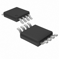
IC SW CAP/DBLR ADJ .125A 8MSOP

LTC1751EMS8

Manufacturer Part Number
LTC1751EMS8
Description
IC SW CAP/DBLR ADJ .125A 8MSOP
Manufacturer
Linear Technology
Type
Switched Capacitor (Charge Pump), Doublerr
Datasheet

Specifications of LTC1751EMS8

Internal Switch(s)
Yes
Synchronous Rectifier
No
Number Of Outputs
1
Voltage - Output
Adjustable
Current - Output
125mA
Frequency - Switching
800kHz
Voltage - Input
2.5 ~ 5.5 V
Operating Temperature
-40°C ~ 85°C
Mounting Type
Surface Mount
Package / Case
8-MSOP, Micro8™, 8-uMAX, 8-uSOP,
Lead Free Status / RoHS Status
Contains lead / RoHS non-compliant
Power - Output
-

Available stocks

Company
Part Number
Manufacturer
Quantity
Price
Part Number:
LTC1751EMS8
Manufacturer:
LT
Quantity:
10 000
Part Number:
LTC1751EMS8
Manufacturer:
LT
Quantity:
20 000
Part Number:
LTC1751EMS8#PBF
Manufacturer:
LINEAR/凌特
Quantity:
20 000
Part Number:
LTC1751EMS8-3
Manufacturer:
LT
Quantity:
10 000
Part Number:
LTC1751EMS8-3.3
Manufacturer:
LT
Quantity:
10 000
Part Number:
LTC1751EMS8-3.3
Manufacturer:
LINEAR/凌特
Quantity:
20 000
Company:
Part Number:
LTC1751EMS8-3.3#PBF
Quantity:
1 312
Part Number:
LTC1751EMS8-5
Manufacturer:
LT
Quantity:
10 000
Part Number:
LTC1751EMS8-5#PBF
Manufacturer:
LINEAR/凌特
Quantity:
20 000
FEATURES
APPLICATIO S
TYPICAL APPLICATIO
TO 5.5V
2.7V
5V Output Current: 100mA (V
3.3V Output Current: 80mA (V
Ultralow Power: 20 A Quiescent Current
Regulated Output Voltage: 3.3V 4%, 5V 4%, ADJ
No Inductors
Short-Circuit/Thermal Protection
V
800kHz Switching Frequency
Very Low Shutdown Current: <2 A
Shutdown Disconnects Load from V
PowerGood/Undervoltage Output
Adjustable Soft-Start Time
Available in an 8-Pin MSOP Package
Li-Ion Battery Backup Supplies
Local 3V and 5V Conversion
Smart Card Readers
PCMCIA Local 5V Supplies
White LED Backlighting
V
IN
IN
10 F
Range: 2V to 5.5V
C2
OFF ON
Regulated 5V Output from a 2.7V to 5.5V Input
C
C1, C2 = MURATA GRM40X5R106K6.3AJ
FLY
U
= MURATA GRM39X5R105K6.3AJ
3
7
8
4
V
SHDN
SS
GND
IN
LTC1751-5
PGOOD
1751 TA01
V
OUT
C
C
IN
+
IN
U
2
1
6
5
3V)
2.5V)
R1
100k
IN
C
1 F
FLY
PGOOD
C1
10 F
V
5V 4%
I
I
OUT
OUT
OUT
LTC1751/LTC1751-3.3/LTC1751-5
100mA, V
50mA, V
DESCRIPTIO
The LTC
DC converters that produce a regulated output voltage at
up to 100mA. The input voltage range is 2V to 5.5V.
Extremely low operating current (20 A typical with no
load) and low external parts count (one flying capacitor
and two small bypass capacitors at V
them ideally suited for small, battery-powered applica-
tions.
The LTC1751 family operate as Burst Mode
capacitor voltage doublers to achieve ultralow quiescent
current. They have thermal shutdown capability and can
survive a continuous short circuit from V
PGOOD pin on the LTC1751-3.3 and LTC1751-5 indicates
when the output voltage has reached its final value and if
the output has an undervoltage fault condition. The FB pin
of the adjustable LTC1751 can be used to program the
desired output voltage or current. An optional soft-start
capacitor may be used at the SS pin to prevent excessive
inrush current during start-up.
The LTC1751 family is available in an 8-pin MSOP
package.
Burst Mode is a trademark of Linear Technology Corporation.
, LTC and LT are registered trademarks of Linear Technology Corporation.
IN
IN
Micropower, Regulated
2.7V
3V
®
1751 family are micropower charge pump DC/
DC/DC Converters
U
4.9
5.2
5.1
5.0
4.8
2.5
Charge Pump
Output Voltage vs Input Voltage
I
C
C
OUT
FLY
OUT
T
A
= –40 C
= 50mA
3.0
= 1 F
= 10 F
T
A
INPUT VOLTAGE (V)
= 85 C
3.5
T
IN
A
= 25 C
4.0
and V
OUT
4.5
to GND. The
TM
OUT
switched
5.0
) make
1751 TA02
1
5.5

Related parts for LTC1751EMS8

LTC1751EMS8 Summary of contents

Page 1

... An optional soft-start capacitor may be used at the SS pin to prevent excessive inrush current during start-up. The LTC1751 family is available in an 8-pin MSOP package. , LTC and LT are registered trademarks of Linear Technology Corporation. Burst Mode is a trademark of Linear Technology Corporation OUT ...

Page 2

... IN OUT V = 2.7V (Note 5) IN OUT U W ORDER PART NUMBER 8 SS LTC1751EMS8 7 SHDN LTC1751EMS8-3 – LTC1751EMS8-5 MS8 PART MARKING = 160 C/W JA LTKL LTKN LTKP = 10 F unless otherwise noted. OUT MIN TYP MAX 2 4.4 3.17 3.3 3.43 3.17 3.3 3. 2.7 5 ...

Page 3

... Note 1: Absolute Maximum Ratings are those values beyond which the life of a device may be impaired. Note 2: Based on long term current density limitations. Note 3: The LTC1751EMS8-X is guaranteed to meet performance specifications from Specifications over the – operating temperature range are assured by design, characterization and correlation with statistical process controls ...

Page 4

LTC1751/LTC1751-3.3/LTC1751 TYPICAL PERFOR A CE CHARACTERISTICS (LTC1751-3.3) Power Efficiency vs Load Current 100 FLY OUT ...

Page 5

W U TYPICAL PERFOR A CE CHARACTERISTICS (LTC1751-5) Power Efficiency vs Load Current 100 FLY OUT 0.001 ...

Page 6

LTC1751/LTC1751-3.3/LTC1751 PLIFIED BLOCK DIAGRA S PGOOD V OUT V IN GND FB V OUT V IN GND 6 W LTC1751-3.3/LTC1751-5 READY + – – – + – + UNDERV + 2 COMP1 – CHARGE PUMP 3 ...

Page 7

U U APPLICATIO S I FOR ATIO Operation (Refer to Simplified Block Diagrams) The LTC1751 family uses a switched capacitor charge pump to boost regulated output voltage. Regula- IN tion is achieved by sensing the output voltage ...

Page 8

LTC1751/LTC1751-3.3/LTC1751 APPLICATIO S I FOR ATIO Flying Capacitor Selection Warning: A polarized capacitor such as tantalum or aluminum should never be used for the flying capacitor since its voltage can reverse upon start-up of the LTC1751. Low ESR ...

Page 9

U U APPLICATIO S I FOR ATIO There are several ways to reduce output voltage ripple. For applications requiring V to exceed 3.3V or for IN applications requiring < 100mV of peak-to-peak ripple, a larger C capacitor ( ...

Page 10

LTC1751/LTC1751-3.3/LTC1751 APPLICATIO S I FOR ATIO Programming the LTC1751 Output Voltage (FB Pin) While the LTC1751-3.3/LTC1751-5 versions have internal resistive dividers to program the output voltage, the programmable LTC1751 may be set to an arbitrary voltage via an ...

Page 11

... Information furnished by Linear Technology Corporation is believed to be accurate and reliable. However, no responsibility is assumed for its use. Linear Technology Corporation makes no represen- tation that the interconnection of its circuits as described herein will not infringe on existing patent rights. LTC1751/LTC1751-3.3/LTC1751-5 2-Cell NiCd or NiMH to 3.3V with Low Standby Current ...

Page 12

... 50mA Output, SOT-23 Package Q Buck/Boost Charge Pump, I Low Noise, 5V Output or Adjustable LEDS 1751 TA03 0.118 0.004* (3.00 0.102 0.118 0.004** 0.193 0.006 (3.00 0.102) (4.90 0.15 500 2.7V to 10V IN , 2.5V to 5.5V Output RMS = 2. 1751f LT/TP 0401 4K • PRINTED IN USA LINEAR TECHNOLOGY CORPORATION 2000 ...

Related keywords