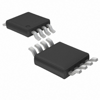
LTC1751EMS8 Linear Technology, LTC1751EMS8 Datasheet - Page 5

LTC1751EMS8
Manufacturer Part Number
LTC1751EMS8
Description
IC SW CAP/DBLR ADJ .125A 8MSOP
Manufacturer
Linear Technology
Type
Switched Capacitor (Charge Pump), Doublerr
Datasheet
1.LTC1751EMS8-5PBF.pdf
(12 pages)
Specifications of LTC1751EMS8
Internal Switch(s)
Yes
Synchronous Rectifier
No
Number Of Outputs
1
Voltage - Output
Adjustable
Current - Output
125mA
Frequency - Switching
800kHz
Voltage - Input
2.5 ~ 5.5 V
Operating Temperature
-40°C ~ 85°C
Mounting Type
Surface Mount
Package / Case
8-MSOP, Micro8™, 8-uMAX, 8-uSOP,
Lead Free Status / RoHS Status
Contains lead / RoHS non-compliant
Power - Output
-
Available stocks
Company
Part Number
Manufacturer
Quantity
Price
Company:
Part Number:
LTC1751EMS8
Manufacturer:
LT
Quantity:
10 000
Part Number:
LTC1751EMS8
Manufacturer:
LT
Quantity:
20 000
Part Number:
LTC1751EMS8#PBF
Manufacturer:
LINEAR/凌特
Quantity:
20 000
Company:
Part Number:
LTC1751EMS8-3
Manufacturer:
LT
Quantity:
10 000
Company:
Part Number:
LTC1751EMS8-3.3
Manufacturer:
LT
Quantity:
10 000
Part Number:
LTC1751EMS8-3.3
Manufacturer:
LINEAR/凌特
Quantity:
20 000
Company:
Part Number:
LTC1751EMS8-5
Manufacturer:
LT
Quantity:
10 000
Part Number:
LTC1751EMS8-5#PBF
Manufacturer:
LINEAR/凌特
Quantity:
20 000
TYPICAL PERFOR A CE CHARACTERISTICS
(LTC1751-5)
PGOOD
PI FU CTIO S
2V/DIV
5V/DIV
2V/DIV
PGOOD (Pin 1) (LTC1751-3.3/LTC1751-5): Output Volt-
age Status Indicator. On start-up, this open-drain pin re-
mains low until the output voltage, V
(typ) of its final value. Once V
high-Z. If, due to a fault condition, V
its correct regulation level, PGOOD pulls low. PGOOD may
be pulled up through an external resistor to any appropri-
ate reference level.
FB (Pin 1) (LTC1751): The voltage on this pin is compared
to the internal reference voltage (1.205V) by the error
comparator to keep the output in regulation. An external
resistor divider is required between V
gram the output voltage.
V
mance, V
ESR capacitor as close to the pin as possible .
SHDN
V
OUT
OUT
U
Start-Up
C
(Pin 2): Regulated Output Voltage. For best perfor-
SS
= 10nF
OUT
U
should be bypassed with a 6.8 F (min) low
2ms/DIV
100
90
80
70
60
40
30
20
10
50
0.001
0
U
Power Efficiency vs Load Current
T
C
C
A
FLY
OUT
= 25 C
= 1 F
= 10 F
0.01
W
OUT
LOAD CURRENT (mA)
1751 G13
is valid, PGOOD becomes
0.1
U
OUT
OUT
AC COUPLED
falls 7% (typ) below
OUT
1
50mV/DIV
V
V
V
IN
IN
IN
, is within 4.5%
= 2.7V
= 4.1V
= 5.5V
and FB to pro-
V
OUT
10
Output Ripple
V
I
C
OUT
1751 G11
IN
OUT
= 3V
= 100mA
= 10 F
100
LTC1751/LTC1751-3.3/LTC1751-5
5 s/DIV
V
with a 6.8 F (min) low ESR capacitor.
GND (Pin 4): Ground. Should be tied to a ground plane for
best performance.
C
C
SHDN (Pin 7): Active Low Shutdown Input. A low on
SHDN disables the device. SHDN must not be allowed to
float.
SS (Pin 8): Soft-Start Programming Pin. A capacitor on SS
programs the start-up time of the charge pump so that
large start-up input current is eliminated.
IN
+
–
(PIN 6): Flying Capacitor Positive Terminal.
(Pin 5): Flying Capacitor Negative Terminal.
(Pin 3): Input Supply Voltage. V
200
100
250
150
50
2.0
Short-Circuit Output Current
vs Input Voltage
T
C
A
1751 G14
FLY
= 25 C
2.5
= 1 F
3.0
AC COUPLED
INPUT VOLTAGE (V)
50mA/DIV
50mV/DIV
3.5
V
I
OUT
OUT
4.0
Load Transient Response
V
IN
= 3V
4.5
IN
5.0
1751 G12
should be bypassed
50 s/DIV
5.5
5
1751 G15


