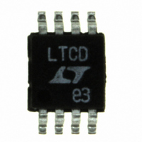
LT1316CMS8#TR Linear Technology, LT1316CMS8#TR Datasheet - Page 10

LT1316CMS8#TR
Manufacturer Part Number
LT1316CMS8#TR
Description
IC CONV DC/DC STEP UP 8MSOP
Manufacturer
Linear Technology
Type
Step-Up (Boost)r
Datasheet
1.LT1316CS8PBF.pdf
(16 pages)
Specifications of LT1316CMS8#TR
Internal Switch(s)
Yes
Synchronous Rectifier
No
Number Of Outputs
1
Voltage - Output
1.23 ~ 30 V
Current - Output
500mA
Voltage - Input
1.5 ~ 12 V
Operating Temperature
0°C ~ 70°C
Mounting Type
Surface Mount
Package / Case
8-MSOP, Micro8™, 8-uMAX, 8-uSOP,
Lead Free Status / RoHS Status
Contains lead / RoHS non-compliant
Power - Output
-
Frequency - Switching
-
Available stocks
Company
Part Number
Manufacturer
Quantity
Price
APPLICATIONS
LT1316
Layout/Input Bypassing
The LT1316’s high speed switching mandates careful
attention to PC board layout. Suggested component place-
ment is shown in Figure 9. The input supply must have low
impedance at AC and the input capacitor should be placed
as indicated in the figure. The value of this capacitor
depends on how close the input supply is to the IC. In
situations where the input supply is more than a few
inches away from the IC, a 47 F to 100 F solid tantalum
bypass capacitor is required. If the input supply is close to
the IC, a 1 F ceramic capacitor can be used instead. The
LT1316 switches current in pulses up to 0.5A, so a low
impedance supply must be available. If the power source
(for example, a 2 AA cell battery) is within 1 or 2 inches of
the IC, the battery itself provides bulk capacitance and the
10
AC COUPLED
100mV/DIV
100mA/DIV
V
OUT
Figure 7. Switching Waveforms for the Circuit
Shown in Figure 7 Without C1. The Output Ripple
Voltage is Approximately 140mV
I
L
U
INFORMATION
U
100 s/DIV
W
P-P
R
SET
1316 F07
Figure 9. Suggested PC Layout
U
C
1
2
3
4
IN
LT1316
1 F ceramic capacitor acts to smooth voltage spikes at
switch turn-on and turn-off. If the power source is far away
from the IC, inductance in the power source leads results
in high impedance at high frequency. A local high capaci-
tance bypass is then required to restore low impedance at
the IC.
Low-Battery Detector
The LT1316 contains an independent low-battery detector
that remains active when the device is shut down. This
detector, actually a hysteretic comparator, has an open
collector output that can sink up to 500 A. The compara-
tor also operates below the switcher’s undervoltage lock-
out threshold, operating until V
1.4V.
8
7
6
5
AC COUPLED
100mV/DIV
100mA/DIV
D
L
V
OUT
+
C
V
I
Figure 8. By Adding C1, Output Ripple Voltage
is Reduced to Less Than 80mV
OUT
OUT
L
1316 F09
GND
V
IN
50 s/DIV
IN
reaches approximately
P-P
1316 F08


