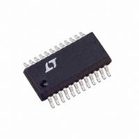
LTC3736EGN-2#PBF Linear Technology, LTC3736EGN-2#PBF Datasheet - Page 7

LTC3736EGN-2#PBF
Manufacturer Part Number
LTC3736EGN-2#PBF
Description
IC CTRLR SW SYNC DUAL 2PH 24SSOP
Manufacturer
Linear Technology
Series
PolyPhase®r
Type
Step-Down (Buck)r
Datasheet
1.LTC3736EGN-2PBF.pdf
(28 pages)
Specifications of LTC3736EGN-2#PBF
Internal Switch(s)
No
Synchronous Rectifier
Yes
Number Of Outputs
2
Voltage - Output
0.6 ~ 9.8 V
Current - Output
1A
Frequency - Switching
550kHz ~ 750kHz
Voltage - Input
2.75 ~ 9.8 V
Operating Temperature
-40°C ~ 85°C
Mounting Type
Surface Mount
Package / Case
24-SSOP
Lead Free Status / RoHS Status
Lead free / RoHS Compliant
Power - Output
-
Available stocks
Company
Part Number
Manufacturer
Quantity
Price
select. For auxiliary winding applications, connect to a
resistor divider from the auxiliary output. To synchronize
with an external clock using the PLL, apply a CMOS compat-
ible clock with a frequency between 250kHz and 850kHz.
To select pulse-skipping operation at light loads, tie this
pin to V
operation, which allows the inductor current to reverse.
When synchronized to an external clock, pulse-skipping
operation is enabled at light loads.
BG1/BG2 (Pins 19, 13/Pins 22, 16): Bottom (NMOS) Gate
Drive Output. These pins drive the gates of the external
N-channel MOSFETs. These pins have an output swing
from PGND to SENSE
SENSE1
Input to Differential Current Comparator. Also powers
the gate drivers. Normally connected to the source of the
external P-channel MOSFET.
PIN FUNCTIONS
FUNCTIONAL DIAGRAM
IN
+
/SENSE2
. Grounding this pin selects forced continuous
+
(Pins 21, 11/Pins 24, 14): Positive
+
.
SYNC/FCB
RUN/SS
PLLLPF
(QFN/SSOP Package)
UNDERVOLTAGE
LOCKOUT
0.6V
0.7μA
–
+
VOLTAGE CONTROLLED
SYNC DETECT
FCB
OSCILLATOR
V
(Common Circuitry)
IN
EXTSS
REFERENCE
VOLTAGE
SHDN
FCB
t
SEC
CLK1
CLK2
= 1ms
C
0.54V
0.6V
V
VIN
REF
R
VIN
DETECTOR
V
V
FB1
FB2
PHASE
SW1/SW2 (Pins 22, 10/Pins 1, 13): Switch Node Con-
nection to Inductor. Also the negative input to differential
peak current comparator and an input to the reverse cur-
rent comparator. Normally connected to the drain of the
external P-channel MOSFETs, the drain of the external
N-channel MOSFET, and the inductor.
IPRG1/IPRG2 (Pins 23, 2/Pins 2, 5): Three-State Pins to
Select Maximum Peak Sense Voltage Threshold. These
pins select the maximum allowed voltage drop between
the SENSE
across the external P-channel MOSFET) for each channel.
Tie to V
respectively.
V
ceives the remotely sensed feedback voltage for its con-
troller from an external resistor divider across the output.
FB1
V
(TO CONTROLLER 1, 2)
IN
+
–
–
+
+
–
/V
FB2
SLOPE
COMP
IN
, GND or fl oat to select 345mV, 167mV, or 240mV,
+
(Pins 24, 7/Pins 3, 10): Feedback Pins. Re-
and SW pins (i.e., the maximum allowed drop
UV1
UV2
INTSS
SLOPE1
SLOPE2
OV1
SHDN
OV2
PGOOD
37362 FD
LTC3736-2
37362fb
7


