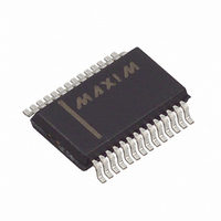
MAX1631EAI+T Maxim Integrated Products, MAX1631EAI+T Datasheet - Page 23

MAX1631EAI+T
Manufacturer Part Number
MAX1631EAI+T
Description
IC PS CTRLR FOR NOTEBOOKS 28SSOP
Manufacturer
Maxim Integrated Products
Type
Step-Down (Buck)r
Datasheet
1.MAX1634CAI.pdf
(29 pages)
Specifications of MAX1631EAI+T
Internal Switch(s)
No
Synchronous Rectifier
Yes
Number Of Outputs
2
Voltage - Output
3.3V, 5V, Adj
Current - Output
4A
Frequency - Switching
200kHz, 300kHz
Voltage - Input
4.2 ~ 30 V
Operating Temperature
-40°C ~ 85°C
Mounting Type
Surface Mount
Package / Case
28-SSOP
Power - Output
762mW
Output Voltage
2.5 V to 5.5 V, 3.3 V, 5 V
Input Voltage
4.2 V to 30 V
Mounting Style
SMD/SMT
Maximum Operating Temperature
+ 85 C
Minimum Operating Temperature
- 40 C
Lead Free Status / RoHS Status
Lead free / RoHS Compliant
where t
and V
This power is dissipated in the MOSFET body diode if
no external Schottky diode is used.
where I
Design Procedure and Input Capacitor Value sections.
Under light loads, the PWM operates in discontinuous
mode, where the inductor current discharges to zero at
some point during the switching cycle. This makes the
inductor current’s AC component high compared to the
load current, which increases core losses and I
es in the output filter capacitors. For best light-load effi-
ciency, use MOSFETs with moderate gate-charge
levels, and use ferrite, MPP, or other low-loss core
material. Avoid powdered-iron cores; even Kool-Mu
(aluminum alloy) is not as good as ferrite.
Good PC board layout is required in order to achieve
specified noise, efficiency, and stability performance.
The PC board layout artist must be given explicit
instructions, preferably a pencil sketch showing the
placement of power-switching components and high-
current routing. See the PC board layout in the
MAX1630 Evaluation Kit manual for examples. A
ground plane is essential for optimum performance. In
most applications, the circuit will be located on a multi-
layer board, and full use of the four or more copper lay-
ers is recommended. Use the top layer for high-current
connections, the bottom layer for quiet connections
(REF, SS, GND), and the inner layers for an uninterrupt-
ed ground plane. Use the following step-by-step guide:
1) Place the high-power components (Figure1, C1, C3,
P(cap) = input capacitor ESR loss = (I
Q1, Q2, D1, L1, and R1) first, with any grounded
connections adjacent.
Priority 1: Minimize current-sense resistor trace
Priority 2: Minimize ground trace lengths in the
Priority 3: Minimize other trace lengths in the high-
FWD
RMS
D
Light-Load Efficiency Considerations
is the diode-conduction time (120ns typical)
is the forward voltage of the diode.
is the input ripple current as calculated in the
lengths and ensure accurate current
sensing with Kelvin connections (Figure 7).
high-current paths (discussed below).
current paths.
Use >5mm-wide traces
C
max length
PC Board Layout Considerations
IN
to high-side MOSFET drain: 10mm
______________________________________________________________________________________
Multi-Output, Low-Noise Power-Supply
Controllers for Notebook Computers
RMS
)
2
x R
2
R loss-
ESR
Ideally, surface-mount power components are butted
up to one another with their ground terminals almost
touching. These high-current grounds are then con-
nected to each other with a wide filled zone of top-layer
copper so they don’t go through vias. The resulting top-
layer “sub-ground-plane” is connected to the normal
inner-layer ground plane at the output ground termi-
nals, which ensures that the IC’s analog ground is
sensing at the supply’s output terminals without interfer-
ence from IR drops and ground noise. Other high-
current paths should also be minimized, but focusing
primarily on short ground and current-sense con-
nections eliminates about 90% of all PC board lay-
out problems (see the PC board layouts in the
MAX1630 Evaluation Kit manual for examples).
2) Place the IC and signal components. Keep the main
3) Use a single-point star ground where the input
Figure 7. Kelvin Connections for the Current-Sense Resistors
switching nodes (LX nodes) away from sensitive
analog components (current-sense traces and REF
capacitor). Place the IC and analog components on
the opposite side of the board from the power-
switching node. Important: the IC must be no far-
ther than 10mm from the current-sense resistors.
Keep the gate-drive traces (DH_, DL_, and BST_)
shorter than 20mm and route them away from CSH_,
CSL_, and REF.
ground trace, power ground (sub-ground-plane),
and normal ground plane meet at the supply’s out-
put ground terminal. Connect both IC ground pins
and all IC bypass capacitors to the normal ground
plane.
Rectifier diode cathode to low-side
MOSFET: 5mm max length
LX node (MOSFETs, rectifier cathode,
inductor): 15mm max length
MAX1630
HIGH CURRENT PATH
SENSE RESISTOR
23


