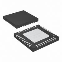
MAX15016AATX+ Maxim Integrated Products, MAX15016AATX+ Datasheet - Page 17

MAX15016AATX+
Manufacturer Part Number
MAX15016AATX+
Description
IC DC/DC CONV 1A 36-TQFN-EP
Manufacturer
Maxim Integrated Products
Type
Step-Down (Buck)r
Datasheet
1.MAX15017AATX.pdf
(26 pages)
Specifications of MAX15016AATX+
Internal Switch(s)
Yes
Synchronous Rectifier
Yes
Number Of Outputs
2
Voltage - Output
1.26 ~ 32 V
Current - Output
1A
Frequency - Switching
135kHz ~ 500kHz
Voltage - Input
4.5 ~ 40 V
Operating Temperature
-40°C ~ 125°C
Mounting Type
Surface Mount
Package / Case
36-TQFN Exposed Pad
Power - Output
2.1W
Lead Free Status / RoHS Status
Lead free / RoHS Compliant
feature a preset output voltage of 5V (MAX1501_A) or
3.3V (MAX1501_B). Alternatively, the output voltage
can be adjusted using an external resistive-divider net-
work connected between LDO_OUT, SET_LDO, and
SGND. See Figure 5.
The RESET output is typically connected to the reset
input of a microprocessor (µP). A µP’s reset input starts
or restarts the µP in a known state. The MAX15014–
MAX15017 supervisory circuits provide the reset logic
to prevent code-execution errors during power-up,
power-down, and brownout conditions. RESET
changes from high to low whenever the monitored volt-
age drops below the RESET threshold voltage. Once
the monitored voltage exceeds its respective RESET
threshold voltage(s), RESET remains low for the RESET
timeout period, then goes high. The RESET timeout
period is adjustable with an external capacitor (C
connected to CT.
The MAX15014–MAX15017 feature thermal shutdown
protection which limits the total power dissipation in the
device and protects it in the event of an extended ther-
mal fault condition. When the die temperature exceeds
+160°C, an internal thermal sensor shuts down the part,
turning off the DC-DC converter and the LDO regulator,
and allowing the IC to cool. After the die temperature
falls by 20°C, the part restarts with a soft-start sequence.
Connect a resistive divider (R3 and R4, see Figures 6
and 7) from OUT to FB to SGND to set the output volt-
age. Choose R3 and R4 so that DC errors due to the FB
input bias current do not affect the output-voltage
setting precision. For the most common output-voltage
settings (3.3V or 5V), R3 values in the 10kΩ range are
adequate. Select R3 first and calculate R4 using the
following equation:
where V
FB
1A, 4.5V to 40V Input Buck Converters with
= 1.235V.
Applications Information
Thermal-Shutdown Protection
R
______________________________________________________________________________________
4
Setting the Output Voltage
=
⎡
⎢
⎣
V
V
OUT
FB
R
3
−
1
⎤
⎥
⎦
RESET Output
50mA Auxiliary LDO Regulators
CT
)
Three key inductor parameters must be specified for
operation with the MAX15014–MAX15017: inductance
value (L), peak inductor current (I
saturation current (I
tance is a function of operating frequency, input-to-out-
put voltage differential, and the peak-to-peak inductor
current (∆I
value while a lower ∆I
value. A lower inductor value minimizes size and cost
and improves large-signal and transient response, but
reduces efficiency due to higher peak currents and
higher peak-to-peak output voltage ripple for the same
output capacitor. On the other hand, higher inductance
increases efficiency by reducing the ∆I
losses due to extra wire turns can exceed the benefit
gained from lower ∆I
inductance is increased without also allowing for larger
inductor dimensions. A good compromise is to choose
∆I
inductor using the following equation:
V
mum for typical conditions. The switching frequency
(f
MAX15016) or 500kHz (MAX15015/MAX15017) and
can vary when synchronized to an external clock (see
the Oscillator/Synchronization Input (SYNC) section).
The ∆I
ple, is worst at the maximum input voltage. See the
Output-Capacitor Selection section to verify that the
worst-case output ripple is acceptable. The inductor
current (I
away during continuous output short circuit. Select an
inductor with an I
maximum peak current limit of 2.6A.
The discontinuous input current of the buck converter
causes large input ripple currents and therefore the
input capacitor must be carefully chosen to keep the
input voltage ripple within design requirements. The
input voltage ripple is comprised of ∆V
the capacitor discharge) and ∆V
ESR of the input capacitor). The total voltage ripple is
the sum of ∆V
tance and ESR required for a specified ripple using the
following equations:
IN
SW
P-P
and V
) is internally fixed at 135kHz (MAX15014/
equal to 40% of the full load current. Calculate the
P-P
OUT
, which reflects the peak-to-peak output rip-
SAT
P-P
) is also important to avoid current run-
). Higher ∆I
Q
are typical values so that efficiency is opti-
and ∆V
L
=
SAT
SAT
V
V
OUT IN
IN
Input-Capacitor Selection
P-P
). The minimum required induc-
ESR
P-P
specification higher than the
×
P-P
(
f
V
SW
levels especially when the
. Calculate the input capaci-
requires a higher inductor
allows for a lower inductor
×
−
V
Inductor Selection
∆
OUT
I
P P
−
ESR
PEAK
)
(caused by the
), and inductor
Q
P-P
(caused by
. Resistive
17


