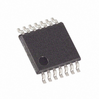
MAX5426AEUD+ Maxim Integrated Products, MAX5426AEUD+ Datasheet - Page 5

MAX5426AEUD+
Manufacturer Part Number
MAX5426AEUD+
Description
IC INSTR AMP PROGR PREC 14-TSSOP
Manufacturer
Maxim Integrated Products
Datasheet
1.MAX5426CEUDT.pdf
(9 pages)
Specifications of MAX5426AEUD+
Applications
*
Mounting Type
Surface Mount
Package / Case
14-TSSOP
Lead Free Status / RoHS Status
Lead free / RoHS Compliant
The MAX5426 is a precision resistor network with low
temperature drift and high accuracy that performs the
same function as a precision resistor array and CMOS
switches. Operationally, this device consists of fixed
resistors and digitally controlled variable resistors that
provide differential gains of 1, 2, 4, and 8 (see
Functional Diagram). The MAX5426 provides gains
accurate to 0.025% (MAX5426A), 0.09% (MAX5426B)
or 0.5% (MAX5426C).
The MAX5426 is ideal for programmable instrumenta-
tion amplifiers. An offset pin is available to apply a DC
offset voltage to the output of the differential amplifier.
Pin CM is the common-mode input voltage and can be
buffered and connected to the common-mode input of
the instrumentation amplifier (usually the shield of the
input cable to reduce the effects of cable capacitance
and leakage).
The MAX5426 features a simple two-bit parallel pro-
gramming interface. D1 and D0 program the gain set-
ting according to the Logic-Control Truth Table (see
Table 1). The digital interface is CMOS/TTL logic com-
patible.
13, 14
PIN
10
11
12
1
2
3
4
5
6
7
8
9
OFFSET
INDIF+
Programmable Instrumentation Amplifiers
D0, D1
NAME
INDIF-
OUT2
OUT1
GND
OUT
V
V
FB2
FB1
CM
DD
SS
_______________________________________________________________________________________
Digital Interface Operation
Detailed Description
Positive Power Supply. Bypass V
Ground
Negative Power Supply. Bypass V
First Stage Positive Input Terminal Resistor. Connect to the inverting terminal of the second input buffer
(see Figure 1).
First Stage Positive Output Terminal Resistor. Connect to the output terminal of the second input buffer.
Second Stage Offset Terminal. Connect to a DC voltage to offset the output of the differential amplifier.
Second Stage Negative Input Terminal Resistor. Connect to the inverting input terminal of the
differential op amp.
Second Stage Positive Input Terminal Resistor. Connect to the noninverting input terminal of the
differential op amp.
Second Stage Output Terminal, Final Output Terminal
First Stage Negative Output Terminal of Resistor. Connect to the output terminal of the first input buffer.
First Stage Negative Input Terminal of Resistor. Connect to the inverting input terminal of the first input
buffer.
Common-Mode Voltage. CM is the input common-mode voltage of the instrumentation amplifier.
Typically varies ±1% of input common-mode voltage.
Digital Inputs. See Table 1.
Precision Resistor Network for
DD
SS
to GND with a 0.1µF capacitor.
to GND with a 0.1µF capacitor.
Figure 3 shows the timing diagram of MAX5426 for two
cases. In case 1, the differential input changes are at
OUT1 and OUT2, while the voltage settling is observed
at FB1 and FB2. The settling time (t
as the time for the output voltage (from the change in
the input) to reach (and stay) within 0.02% of its final
value.
In case 2, the differential inputs (OUT1 and OUT2) are
at constant voltages, while D1 and D0 are varied (for
example from 01 to 10) to make a change in the gain.
No op amps are used in these cases.
Table 1. Logic-Control Truth Table
D1
FUNCTION
0
0
1
1
DIGITAL INPUTS
D0
0
1
0
1
Timing Diagram
Pin Description
SETTLE
GAIN
1
2
4
8
) is defined
5


