KS8999 Micrel Inc, KS8999 Datasheet
KS8999
Specifications of KS8999
Available stocks


Related parts for KS8999

KS8999 Summary of contents
Page 1
... MII port. The additional port is also useful for a public network interfacing. The KS8999 is designed to reside in an unmanaged design not requiring processor intervention. Functional Diagram Micrel Inc. • 2180 Fortune Drive • San Jose, CA 95131 • USA • tel +1 (408) 944-0800 • fax + 1 (408) 474-1000 • http://www.micrel.com ...
Page 2
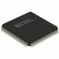
... Available in 208-pin PQFP package Ordering Information Part Number Temp Range KS8999 0°C to +70°C KS8999I –40°C to +85°C KSZ8999 0°C to +70°C KSZ8999I –40°C to +85°C 2 KS8999 Package 208-Pin PQFP 208-Pin PQFP 208-Pin PQFP 208-Pin PQFP KS8999 ...
Page 3
... Correct pin 174 and 175 description 1.09 6/18/02 Correct default to floating for pin 174 Change pin 87 TEST[3] to AUTOMDIX for enable/disable of auto MDI-MDIX function 1.10 2/27/03 Add KS8999I industrial temperature Update non-periodic blinking in Mode 1 of LED[1:9][0] Add MRXD[0] description 1.11 5/12/03 Changed V 1.12 8/29/03 Convert to new format ...
Page 4
... Broadcast Storm Protection......................................................................................................................................22 MII Interface Operation .................................................................................................................................................23 SNI Interface (7-wire) Operation ..................................................................................................................................25 Programmable Features ...............................................................................................................................................25 Priority Schemes.......................................................................................................................................................25 Per Port Method........................................................................................................................................................25 802.1p Method..........................................................................................................................................................25 IPv4 DSCP Method...................................................................................................................................................25 Other Priority Considerations....................................................................................................................................25 VLAN Operation.............................................................................................................................................................26 Station MAC Address (control frames only) ..............................................................................................................27 EEPROM Operation.......................................................................................................................................................27 Optional CPU Interface .................................................................................................................................................28 January 2005 4 KS8999 KS8999 ...
Page 5
... Station MAC Address Registers (all ports –MAC control frames only) ....................................................................38 Absolute Maximum Ratings .........................................................................................................................................39 Operating Ratings .........................................................................................................................................................39 Electrical Characteristics .............................................................................................................................................39 Timing Diagrams ...........................................................................................................................................................41 Reference Circuits.........................................................................................................................................................47 Reset Reference Circuit................................................................................................................................................47 4B/5B Coding.................................................................................................................................................................49 MLT3 Coding..................................................................................................................................................................50 MAC Frame ....................................................................................................................................................................50 Selection of Isolation Transformers............................................................................................................................51 Selection of Reference Oscillator/Crystal ..................................................................................................................51 Package Information .....................................................................................................................................................52 January 2005 5 KS8999 KS8999 ...
Page 6
... Micrel, Inc. System Level Applications The KS8999 can be configured to fit either in an eight port 10/100 application nine port 10/100 network interface with an extra MII/7-wire port. This MII/7-wire port can be connected to an external processor and used for routing purposes or public January 2005 network access ...
Page 7
... Micrel, Inc. Pin Configuration January 2005 208-Pin PQFP (PQ) 7 KS8999 KS8999 ...
Page 8
... Physical receive signal + (differential Physical receive signal - (differential) GND Ground for transmit circuitry O 5 Physical transmit signal + (differential Physical transmit signal - (differential) GND Analog ground Pwr 2.0V for transmit circuitry Pwr 2.0V for transmit circuitry GND Ground for transmit circuitry 8 KS8999 KS8999 ...
Page 9
... Fiber signal detect GND Ground for clock recovery circuit GND Ground for clock recovery circuit Pwr 2.0V for clock recovery circuit Pwr 2.0V for clock recovery circuit GND Ground for clock recovery circuit GND Ground for clock recovery circuit 9 KS8999 KS8999 ...
Page 10
... Ground for digital circuitry Pwr 2.0V for core digital circuitry Ipd Built in self test –tie low for normal operation I Reset –active low Ipu/O 1 LED indicator 3 Ipu/O 1 LED indicator 2 Ipu/O 1 LED indicator 1 Ipu/O 1 LED indicator 0 Ipu/O 2 LED indicator 3 Ipu/O 2 LED indicator 2 10 KS8999 KS8999 ...
Page 11
... LED indicator 3 Ipu/O 7 LED indicator 2 Ipu/O 7 LED indicator 1 Pwr 2.0V, 2.5V or 3.3V for I/O circuitry Ipu/O 7 LED indicator 0 Ipu/O 8 LED indicator 3 Ipu/O 8 LED indicator 2 Ipu/O 8 LED indicator 1 Ipu/O 8 LED indicator 0 GND Ground for digital circuitry GND Ground for digital circuitry 11 KS8999 KS8999 ...
Page 12
... Pwr 2.0V for clock recovery circuit GND Ground for clock recovery circuit GND Ground for clock recovery circuit Ipd 1 Fiber signal detect Ipd 2 Fiber signal detect Ipd 3 Fiber signal detect Ipd 4 Fiber signal detect Pwr 2.0V for equalizer 12 KS8999 KS8999 ...
Page 13
... Physical transmit signal - (differential) Pwr 2.0V for transmit circuitry Pwr 2.0V for transmit circuitry O 2 Physical transmit signal + (differential Physical transmit signal - (differential) GND Ground for transmit circuitry I 2 Physical receive signal + (differential Physical receive signal - (differential) GND Analog ground 13 KS8999 KS8999 ...
Page 14
... Mode 2: Collision (on = collision/off = no collision) Mode 3: Speed (on = 100/off = 10) L Output (after reset) Mode 0: Full Duplex (on = full/off = half) Mode 1: Full Duplex (on = full/off = half) Mode 2: Full Duplex (on = full/off = half) Mode 3: Reserved 14 KS8999 KS8999 ...
Page 15
... Used for factory testing Programs auto-negotiation on port Disable auto-negotiation, F/U = Enable auto-negotiation (default) Programs auto-negotiation on port Disable auto-negotiation, F/U = Enable auto-negotiation (default) Programs auto-negotiation on port Disable auto-negotiation, F/U = Enable auto-negotiation (default) Programs auto-negotiation on port Disable auto-negotiation, F/U = Enable auto-negotiation (default) 15 KS8999 KS8999 ...
Page 16
... Programs back-off aggressiveness for half-duplex mode D = Less aggressive back-off, F/U = More aggressive back-off (default) Programs retries for frames that encounter collisions Drop frame after 16 collisions, F/U = Continue sending frame regardless of the number of collisions (default) Reserved – use float configuration 16 KS8999 KS8999 ...
Page 17
... I/O Serial data for EEPROM L System reset H Factory test input –tie low for normal operation H Factory test input –tie low for normal operation H Factory test input –leave open for normal operation H Factory test output –leave open for normal operation 17 KS8999 KS8999 ...
Page 18
... Ground for transmit circuitry 2.0V for clock recovery circuitry Ground for clock recovery 2.0V for phase locked loop circuitry Ground for phase locked loop circuitry Analog ground 2.0V for core digital circuitry 2.0V, 2.5V or 3.3V for I/O circuitry Ground for digital circuitry 18 KS8999 KS8999 ...
Page 19
... Finally, the NRZ serial data is provided as the input data to the MAC. PLL Clock Synthesizer The KS8999 generates 125MHz, 62.5MHz, 25MHz and 10MHz clocks for system timing. Internal clocks are generated from an external 25MHz crystal. Scrambler/De-scrambler (100BaseTX only) The purpose of the scrambler is to spread the power spectrum of the signal in order to reduce EMI and baseline wander ...
Page 20
... Power Save Mode The KS8999 will turn off everything except for the Energy Detect and PLL circuits when the cable is not installed on an individual port basis. In other words, the KS8999 will shutdown most of the internal circuits to save power if there is no link. ...
Page 21
... If the DA look-up results is a “match”, the KS8999 will use the destination port information to determine where the packet goes. • If the DA look-up result is a “miss”, the KS8999 will forward the packet to all other ports except the port that received the packet. ...
Page 22
... The KS8999 will flow control a port, which just received a packet, if the destination port resource is being used up. The KS8999 will issue a flow control frame (XOFF), containing the maximum pause time defined in IEEE standard 802.3x. Once the resource is freed up, the KS8999 will send out the other flow control frame (XON) with zero pause time ...
Page 23
... Micrel, Inc. MII Interface Operation The MII (Media Independent Interface) operates in either a MAC or PHY mode. In the MAC mode, the KS8999 MII acts like a MAC and in the PHY mode, it acts like a PHY device. This interface is specified by the IEEE 802.3 committee and provides a common interface between physical layer and MAC layer devices. There are two distinct groups, one being for transmission and the other for receiving ...
Page 24
... Micrel, Inc. Note that the signal MRXER is not provided on the MII interface for the KS8999 for PHY mode operation and MTXER is not represented for MAC mode. Normally this would indicate a receive / transmit error coming from the physical layer /MAC device, but is not appropriate for this configuration. If the connecting device has a MRXER pin, this should be tied low on the other device for reverse has a MTXER pin in the forward mode it should also be tied low on the other device ...
Page 25
... Programmable Features Priority Schemes The KS8999 can determine priority through three different means at the ingress point. The first method is a simple per port method, the second is via the 802.1p frame tag and the third is by viewing the DSCP (TOS) field in the IPv4 header ...
Page 26
... Enable Port 802.1p Priority: Uses the 802.1p priority tag (3 bits) to determine frame priority Priority Classification: Determines which tag values have high priority Per Port Priority Enable Port Priority: Determines which ports have high or low priority traffic Table 3. Priority Control 26 KS8999 KS8999 ...
Page 27
... The actual data that traverses the serial line changes during the clock low time. The KS8999 EEPROM interface is compatible with the Atmel AT24C01A part. Address A0, A1 and A2 are fixed to 000. Further timing and data sequences can be found in the Atmel AT24C01A specification. ...
Page 28
... The processor needs to supply the exact number of clock cycles and data bits to program the KS8999 properly. KS8999 won’t start until all of the registers are programmed. Bits are loaded from high order (bit 7) to low order (bit 0) starting with register 0 and finishing with register 53 ...
Page 29
... Insert VLAN tags for port 1 if non-existent 1 = Enable 0 = Disable 4 1 Strip VLAN tags for port 1 if existent 1 = Enable 0 = Disable 4 0 Enable high and low output priority queues for port Enable 0 = Disable January 2005 29 KS8999 Default (chip) Value 0x55 0x99 0000 KS8999 ...
Page 30
... TOS priority classification enable for port Enable 0 = Disable 7 4 802.1p priority classification enable for port Enable 0 = Disable 7 3 Port based priority classification for port High priority 0 = Low priority 7 2 Insert VLAN tags for port 4 if non-existent 1 = Enable 0 = Disable January 2005 30 KS8999 Default (chip) Value KS8999 ...
Page 31
... Enable high and low output priority queues for port Enable 0 = Disable Port 7 Control Register 10 7-6 Reserved –set to zero 10 5 TOS priority classification enable for port Enable 0 = Disable 10 4 802.1p priority classification enable for port Enable 0 = Disable January 2005 31 KS8999 Default (chip) Value KS8999 ...
Page 32
... Strip VLAN tags for port 9 if existent 1 = Enable 0 = Disable 12 0 Enable high and low output priority queues for port Enable 0 = Disable Port 1 VLAN Mask Register 13 7 Port 9 inclusion 1 = Port 9 in the same VLAN as port Port 9 not in the same VLAN as port 1 January 2005 32 KS8999 Default (chip) Value KS8999 ...
Page 33
... Port 9 not in the same VLAN as port Port 8 inclusion 1 = Port 8 in the same VLAN as port Port 8 not in the same VLAN as port Port 7 inclusion 1 = Port 7 in the same VLAN as port Port 7 not in the same VLAN as port 3 January 2005 33 KS8999 Default (chip) Value KS8999 ...
Page 34
... Port 7 not in the same VLAN as port Port 6 inclusion 1 = Port 6 in the same VLAN as port Port 6 not in the same VLAN as port Port 4 inclusion 1 = Port 4 in the same VLAN as port Port 4 not in the same VLAN as port 5 January 2005 34 KS8999 Default (chip) Value KS8999 ...
Page 35
... Port 4 not in the same VLAN as port Port 3 inclusion 1 = Port 3 in the same VLAN as port Port 3 not in the same VLAN as port Port 2 inclusion 1 = Port 2 in the same VLAN as port Port 2 not in the same VLAN as port 7 January 2005 35 KS8999 Default (chip) Value KS8999 ...
Page 36
... Port 2 in the same VLAN as port Port 2 not in the same VLAN as port Port 1 inclusion 1 = Port 1 in the same VLAN as port Port 1 not in the same VLAN as port 9 Port 1 VLAN Tag Insertion Value Registers 22 7-5 User priority [2: CFI January 2005 36 KS8999 Default (chip) Value 000 0 KS8999 ...
Page 37
... Port 8 VLAN Tag Insertion Value Registers 36 7-5 User priority [2: CFI 36 3-0 VID [11:8] 37 7-0 VID [7:0] January 2005 37 KS8999 Default (chip) Value 0x0 0x00 000 0 0x0 0x00 000 0 0x0 0x00 000 0 0x0 0x00 000 0 0x0 0x00 000 0 0x0 0x00 000 0 0x0 0x00 000 0 0x0 0x00 KS8999 ...
Page 38
... MAC address [39:32] 50 7-0 MAC address [31:24] 51 7-0 MAC address [23:16] 52 7-0 MAC address [15:8] 53 7-0 MAC address [7:0] January 2005 38 KS8999 Default (chip) Value 000 0 0x0 0x00 0x00 0x00 0x00 0x00 0x00 0x00 0x00 0x00 0x00 0x40 0x05 0x43 0x5E 0xFE KS8999 ...
Page 39
... DD PLLTX ............................................. –0.5V to +3.8V DDIO Input Voltage ......................................... –0.5V to +4.0V Output Voltage ...................................... –0.5V to +4.0V Lead Temperature (soldering, 10 sec) ................ 270°C Storage Temperature (T ) .................. –55°C to +150°C S Electrical Characteristics (KS8999 2.0V to 2.3V 0°C to +70°; unless noted Symbol Parameter V Supply Voltage DD Supply Current (including TX output driver current) 100BaseTX Operation— ...
Page 40
... Transmit (measured differentially after 1:1 transformer) Peak Differential Output Voltage V P Jitters Added Rise/Fall Times January 2005 Condition Peak-to-peak 5MHz square wave 50Ωfrom each output 50Ωfrom each output KS8999 Min Typ Max Units ±0 0.75 V 0.7 1.4 ns 400 mV 2.3 V ±3 KS8999 ...
Page 41
... Clock Cycle CYC t Output Valid OV January 2005 Figure 7. EEPROM Input Timing Min 16384 20 20 Table 5. EEPROM Input Timing Parameters Figure 8. EEPROM Output Timing Min 16384 4096 4112 Table 6. EEPROM Output Timing Parameters 41 Typ Max Units Typ Max Units ns 4128 ns KS8999 KS8999 ...
Page 42
... Clock Cycle CYC t Output Valid OV January 2005 Figure 9. SNI (7-wire) Input Timing Min 10 0 Table 7. SNI (7-wire) Input Parameters Figure 10. SNI (7-wire) Output Timing Min 0 Table 8. SNI (7-wire) Output Timing Parameters 42 Typ Max Units 100 Typ Max Units 100 KS8999 KS8999 ...
Page 43
... Figure 11. KS8999 PHY Mode―Data Sent from External MAC Controller to KS8999 Symbol Parameter t Clock Cycle (100BaseT) CYC t Clock Cycle (10BaseT) CYC t Set-Up Time S T Hold Time H Table 9. MII Timing in KS8999 PHY and MAC Mode Timing Parameters January 2005 Figure 12. KS8999 PHY Mode Receive Timing Min Typ Max Units 40 ns 400 ns ns ...
Page 44
... Micrel, Inc. Figure 13. KS8999 PHY Mode―Data Sent from KS8999 PHY Mode to External MAC Controller Symbol Parameter t Clock Cycle (100BaseT) CYC t Clock Cycle (10BaseT) CYC t Output Valid OV Table 10. KS8999 PHY Mode Transmit Timing Parameters January 2005 Figure 14 KS8999 PHY Mode Transmit Timing ...
Page 45
... Micrel, Inc. Figure 15. KS8999 MAC Mode―Data Sent from External PHY Device to KS8999 Symbol Parameter t Clock Cycle (100BaseT) CYC t Clock Cycle (10BaseT) CYC t Output Valid S t Output Valid H Table 11. KS8999 PHY Mode Transmit Timing Parameters January 2005 Figure 16. KS8999 MAC Mode Receive Timing ...
Page 46
... Micrel, Inc. Figure 17. KS8999 MAC Mode Timing―Data Sent from KS8999 MAC mode to External PHY Device Symbol Parameter t Clock Cycle (100BaseT) CYC t Clock Cycle (10BaseT) CYC t Output Valid OV Table 12. KS8999 MAC Mode Transmit Timing Parameters January 2005 Figure 18. KS8999 MAC Mode Transit Timing ...
Page 47
... See “I/O Description” section for pull-up/pull-down and float information. Reset Reference Circuit Micrel recommended the following discrete reset circuit as shown in Figure 20 when powering up the KS8999 device. For the application where the reset circuit signal comes from another device (e.g., CPU, FPGA, etc), we recommend the reset circuit as shown in Figure 21 ...
Page 48
... Micrel, Inc. Figure 21. Recommended Circuit for Interfacing with CPU/FPGA Reset At power-on-reset and D1 provide the necessary ramp rise time to reset the KS8999 device. The reset out from CPU/FPGA provides warm reset after power up also recommended to power up the VDD core voltage earlier than VDDIO voltage. At worst case, the both VDD core and VDDIO voltages should come up at the same time ...
Page 49
... Data value D Data value E Data value F Idle Start delimiter part 1 Start delimiter part 2 End delimiter part 1 End delimiter part 2 Transmit error Invalid code Invalid code Invalid code Invalid code Invalid code Invalid code Invalid code Invalid code Invalid code Invalid code KS8999 ...
Page 50
... January 2005 Figure 20. MLT3 Coding Description Preamble and Start of Frame Delimiter 48-bit Destination MAC Address 48-bit Source MAC Address Frame Length Higher Layer Protocol and Frame Data 32-bit Cyclical Redundancy Check End of Stream Delimiter Inter Frame Idles Table 14. MAC Frame 50 KS8999 KS8999 ...
Page 51
... Yes 4 Delta Table 15. Qualified Magnetics Vendor Lists 51 Test Condition 100mV, 100 KHz, 8mA 1MHz (min.) 0MHz to 65MHz Test Condition MHz ppm ps(pk-pk) Single Port Auto MDIX Part H1102 Yes S558-5999-U7 Yes PT163020 Yes HB726 Yes LF8505 Yes KS8999 Number of Ports KS8999 ...
Page 52
... Micrel, Inc. Package Information January 2005 208-Pin PQFP (PQ) 52 KS8999 KS8999 ...
Page 53
... A Purchaser’s use or sale of Micrel Products for use in life support appliances, devices or systems is a Purchaser’s own risk and Purchaser agrees to fully indemnify Micrel for any damages resulting from such use or sale. January 2005 © 2003 Micrel, Incorporated. 53 KS8999 KS8999 ...