AFBR-57J5APZ Avago Technologies US Inc., AFBR-57J5APZ Datasheet - Page 2
AFBR-57J5APZ
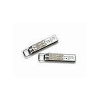
Manufacturer Part Number
AFBR-57J5APZ
Description
TXRX OPT SFP DGTL 850NM IND
Manufacturer
Avago Technologies US Inc.
Series
-r
Datasheet
1.AFBR-57J5APZ.pdf
(18 pages)
Specifications of AFBR-57J5APZ
Wavelength
850nm
Data Rate
3.072Gbps
Applications
General Purpose
Voltage - Supply
2.97 V ~ 3.63 V
Connector Type
LC Duplex
Mounting Type
SFP
Product
Transceiver
Maximum Rise Time
0.1 ns/0.2 ns
Maximum Fall Time
0.1 ns/0.2 ns
Pulse Width Distortion
0.08 ns (Max)/0.065 ns (Max)
Operating Supply Voltage
2.97 V to 3.63 V
Maximum Operating Temperature
+ 85 C
Minimum Operating Temperature
- 40 C
Package / Case
SFP
Lead Free Status / RoHS Status
Lead free / RoHS Compliant
Lead Free Status / RoHS Status
Lead free / RoHS Compliant, Lead free / RoHS Compliant


Digital Diagnostic Interface and Serial Identification
The 2-wire serial interface is based on ATMEL AT24C01A
series EEPROM protocol and signaling detail. Conven-
tional EEPROM memory, bytes 0-255 at memory address
0xA0, is organized in compliance with INF-8074. New
digital diagnostic information, bytes 0-255 at memory
address 0xA2, is compliant to SFF-8472. The new diag-
nostic information provides the opportunity for Predic-
tive Failure Identification, Compliance Prediction, Fault
Isolation and Component Monitoring.
Transmitter Section
The transmitter section includes consists of the Transmit-
ter Optical SubAssembly (TOSA) and laser driver circuitry.
The TOSA, containing an 850nm VCSEL (Vertical Cavity
Surface Emitting Laser) light source, is located at the
optical interface and mates with the LC optical connector.
The TOSA is driven by a custom IC which uses the
incoming differential high speed logic signal to modulate
the laser diode driver current. This Tx laser driver circuit
regulates the optical power at a constant level provided
the incoming data pattern is dc balanced (8B/10B code,
for example).
Transmit Disable (Tx_Disable)
The AFBR-57J5APZ accepts a TTL and CMOS compatible
transmit disable control signal input (pin 3) which shuts
down the transmitter optical output. A high signal im-
plements this function while a low signal allows normal
transceiver operation. In the event of a fault (e.g. eye
safety circuit activated), cycling this control signal resets
the module as depicted in Figure 4. An internal pull up
resistor disables the transceiver transmitter until the host
pulls the input low. Host systems should allow a 10ms
interval between successive assertions of this control
signal. Tx_Disable can also be asserted via the two-
wire serial interface (address A2h, byte 110, bit 6) and
monitored (address A2h, byte 110, bit 7).
Figure 1. Transceiver Functional Diagram
2
Light from Fiber
Optical Interface
Light to Fiber
Receiver
Transmitter
Photo-Detector
VCSEL
CONTROLLER
EEPROM
Amplification
Quantization
&
Laser Driver &
Safety Circuit
EEPROM
Electrical Interface
TD+ (Transmit Data)
TD- (Transmit Data)
TX_FAULT
TX_DISABLE
Rate Select
RD+ (Receive Data)
RD- (Receive Data)
Rx Loss Of Signal
MOD-DEF1 (SCL)
MOD-DEF2 (SDA)
MOD-DEF0
The contents of A2h, byte 110, bit 6 are logic OR’d with
hardware Tx_Disable (pin 3) to control transmitter
operation..
Transmit Fault (Tx_Fault)
A catastrophic laser fault will activate the transmitter
signal, TX_FAULT, and disable the laser. This signal is
an open collector output (pull-up required on the host
board). A low signal indicates normal laser operation
and a high signal indicates a fault. The TX_FAULT will
be latched high when a laser fault occurs and is cleared
by toggling the TX_DISABLE input or power cycling the
transceiver. The transmitter fault condition can also be
monitored via the two-wire serial interface (address A2,
byte 110, bit 2).
Eye Safety Circuit
The AFBR-57J5APZ provides Class 1 (single fault tolerant)
eye safety by design and has been tested for compliance
with the requirements listed in Table 1. The eye safety
circuit continuously monitors the optical output power
level and will disable the transmitter upon detecting an
unsafe condition beyond the scope of Class 1 certifica-
tion. Such unsafe conditions can be due to inputs from
the host board (Vcc fluctuation, unbalanced code) or a
fault within the transceiver.
Receiver Section
The receiver section includes the Receiver Optical Sub-
Assembly (ROSA) and the amplification/quantization
circuitry. The ROSA, containing a PIN photodiode and
custom transimpedance amplifier, is located at the
optical interface and mates with the LC optical connector.
The ROSA output is fed to a custom IC that provides post-
amplification and quantization.
Related parts for AFBR-57J5APZ
Image
Part Number
Description
Manufacturer
Datasheet
Request
R

Part Number:
Description:
TXRX OPT OC3 MTRJ SFF 2X5DIP
Manufacturer:
Avago Technologies US Inc.
Datasheet:

Part Number:
Description:
TXRX ETHERNET 125MBD MMF 2X5
Manufacturer:
Avago Technologies US Inc.
Datasheet:

Part Number:
Description:
650nm FE Transceiver Eval Kit
Manufacturer:
Avago Technologies US Inc.
Datasheet:

Part Number:
Description:
TXRX OPT SFF 4/2/1GBD 2X7
Manufacturer:
Avago Technologies US Inc.
Datasheet:

Part Number:
Description:
TXRX OPT SFP 4/2/1GBD 850NM
Manufacturer:
Avago Technologies US Inc.
Datasheet:

Part Number:
Description:
TXRX OPT XFP 10GB/S 850NM
Manufacturer:
Avago Technologies US Inc.
Datasheet:

Part Number:
Description:
TXRX OPT 1X9 100MBPS ST EXT TEMP
Manufacturer:
Avago Technologies US Inc.
Datasheet:

Part Number:
Description:
TXRX OPT 1X9 100MBPS SC EXT TEMP
Manufacturer:
Avago Technologies US Inc.
Datasheet:

Part Number:
Description:
TXRX OPT 1X9 100MBPS DUPLEX SC
Manufacturer:
Avago Technologies US Inc.
Datasheet:

Part Number:
Description:
TXRX OPT 1X9 100MBPS DUPLEX ST
Manufacturer:
Avago Technologies US Inc.
Datasheet:

Part Number:
Description:
OPTOCOUPLER GATE DRV 2A 16-SOIC
Manufacturer:
Avago Technologies US Inc.
Datasheet:
Part Number:
Description:
OPTOCOUPLER 2CH 2.5A 16-SOIC
Manufacturer:
Avago Technologies US Inc.
Datasheet:

Part Number:
Description:
OPTOCOUPLER GATE DRV 0.4A 16SOIC
Manufacturer:
Avago Technologies US Inc.
Datasheet:

Part Number:
Description:
OPTOCOUPLER 2.0A 250KHZ 8-DIP
Manufacturer:
Avago Technologies US Inc.
Datasheet:

Part Number:
Description:
OPTOCOUPLER 2.0A 250KHZ GW 8-SMD
Manufacturer:
Avago Technologies US Inc.
Datasheet: