LTM4609MPV#PBF Linear Technology, LTM4609MPV#PBF Datasheet - Page 9
LTM4609MPV#PBF
Manufacturer Part Number
LTM4609MPV#PBF
Description
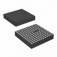
IC UMODULE BUCK-BOOST 141-LGA
Manufacturer
Linear Technology
Series
µModuler
Type
Point of Load (POL) Non-Isolatedr
Datasheet
1.LTM4609EVPBF.pdf
(26 pages)
Specifications of LTM4609MPV#PBF
Design Resources
LTM4609 Spice Model
Output
0.8 ~ 34 V
Number Of Outputs
1
Power (watts)
136W
Mounting Type
Surface Mount
Voltage - Input
4.5 ~ 36 V
Package / Case
141-LGA
1st Output
0.8 ~ 34 VDC @ 4A
Size / Dimension
0.59" L x 0.59" W x 0.11" H (15mm x 15mm x 2.8mm)
Power (watts) - Rated
136W
Operating Temperature
-40°C ~ 85°C
Efficiency
98%
Lead Free Status / RoHS Status
Lead free / RoHS Compliant
3rd Output
-
2nd Output
-
Available stocks
Company
Part Number
Manufacturer
Quantity
Price


OPERATION
APPLICATIONS INFORMATION
Power Module Description
The LTM4609 is a non-isolated buck-boost DC/DC power
supply. It can deliver a wide range output voltage from
0.8V to 34V over a wide input range from 4.5V to 36V,
by only adding the sensing resistor, inductor and some
external input and output capacitors. It provides precisely
regulated output voltage programmable via one external
resistor. The typical application schematic is shown in
Figure 18.
The LTM4609 has an integrated current mode buck-boost
controller, ultralow R
and integrated Schottky diodes. With current mode control
and internal feedback loop compensation, the LTM4609
module has suffi cient stability margins and good transient
performance under a wide range of operating conditions
and with a wide range of output capacitors. The operating
frequency of the LTM4609 can be adjusted from 200kHz
to 400kHz by setting the voltage on the PLLFLTR pin.
The typical LTM4609 application circuit is shown in
Figure 18. External component selection is primarily
determined by the maximum load current and output
voltage. Refer to Table 3 for specifi c external capacitor
requirements for a particular application.
Output Voltage Programming
The PWM controller has an internal 0.8V reference voltage.
As shown in the Block Diagram, a 100k internal feedback
resistor connects V
resistor R
the output voltage:
Table 1. R
V
V
R
R
OUT
OUT
FB
FB
V
OUT
8.66k 7.15k 5.62k
Open
0.8V
10V
= 0.8V •
FB
FB
Resistor (0.5%) vs Output Voltage
from the V
115k
1.5V
12V
100k + R
47.5k
OUT
2.5V
15V
DS(ON)
R
FB
FB
and V
32.4k 19.1k
5.23k 4.12k
pin to the SGND pin programs
3.3V
16V
FB
FETs with fast switching speed
FB
20V
pins together. Adding a
5V
15.4k
3.4k
24V
6V
2.74k 2.37k
11k
30V
8V
9.76k
34V
9V
Alternatively, its frequency can be synchronized by the
input clock signal from the PLLIN pin. The typical switch-
ing frequency is 400kHz.
The Burst Mode
enabled at light loads to improve effi ciency, while the forced
continuous mode and discontinuous mode operations are
used for constant frequency applications. Foldback current
limiting is activated in an overcurrent condition as V
drops. Internal overvoltage and undervoltage compara-
tors pull the open-drain PGOOD output low if the output
feedback voltage exits the ±7.5% window around the
regulation point. Pulling the RUN pin below 1.6V forces
the controller into its shutdown state.
If an external bias supply is applied on the EXTV
an effi ciency improvement will occur due to the reduced
power loss in the internal linear regulator. This is especially
true at the higher end of the input voltage range.
Operation Frequency Selection
The LTM4609 uses current mode control architecture at
constant switching frequency, which is determined by the
internal oscillator’s capacitor. This internal capacitor is
charged by a fi xed current plus an additional current that
is proportional to the voltage applied to the PLLFLTR pin.
The PLLFLTR pin can be grounded to lower the frequency
to 200kHz or tied to 2.4V to yield approximately 400kHz.
When PLLFLTR is left open, the PLLFLTR pin goes low,
forcing the oscillator to its minimum frequency.
A graph for the voltage applied to the PLLFLTR pin vs
frequency is given in Figure 2. As the operating frequency
increases, the gate charge losses will be higher, thus the
effi ciency is lower. The maximum switching frequency is
approximately 400kHz.
FREQUENCY SYNCHRONIZATION
The LTM4609 can also be synchronized to an external
source via the PLLIN pin instead of adjusting the voltage on
the PLLFLTR pin directly. The power module has a phase-
®
and skip-cycle mode operations can be
LTM4609
CC
pin, then
4609fb
9
FB
Related parts for LTM4609MPV#PBF
Image
Part Number
Description
Manufacturer
Datasheet
Request
R

Part Number:
Description:
CD ROM LINEARVIEW DATASHEETS
Manufacturer:
Linear Technology

Part Number:
Description:
Standalone Linear Li-Ion Battery Charger with Thermal Regulation in ThinSOT
Manufacturer:
Linear Technology Corporation
Datasheet:
Part Number:
Description:
Low noise, high frequency, 8th order linear phase lowpass filter
Manufacturer:
Linear Technology Corporation
Datasheet:
Part Number:
Description:
Manufacturer:
Linear Technology Corporation
Datasheet:
Part Number:
Description:
Manufacturer:
Linear Technology Corporation
Datasheet:
Part Number:
Description:
Manufacturer:
Linear Technology Corporation
Datasheet:
Part Number:
Description:
Manufacturer:
Linear Technology Corporation
Datasheet:
Part Number:
Description:
Manufacturer:
Linear Technology Corporation
Datasheet:
Part Number:
Description:
Manufacturer:
Linear Technology Corporation
Datasheet:
Part Number:
Description:
Manufacturer:
Linear Technology Corporation
Datasheet:
Part Number:
Description:
Dual and Quad, JFET Input Precision High Speed Op Amps
Manufacturer:
Linear Technology Corporation
Datasheet:
Part Number:
Description:
Manufacturer:
Linear Technology Corporation
Datasheet:
Part Number:
Description:
1, 2, 6 and 8 Channel, 10-Bit Serial I/O Data Acquisition Systems
Manufacturer:
Linear Technology Corporation
Datasheet:
Part Number:
Description:
Manufacturer:
Linear Technology Corporation
Datasheet:
Part Number:
Description:
Universal dual filter building block
Manufacturer:
Linear Technology Corporation
Datasheet: