LMZ14201TZ-ADJ/NOPB National Semiconductor, LMZ14201TZ-ADJ/NOPB Datasheet - Page 10
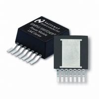
LMZ14201TZ-ADJ/NOPB
Manufacturer Part Number
LMZ14201TZ-ADJ/NOPB
Description
IC BUCK SYNC ADJ 1A TO-PMOD-7
Manufacturer
National Semiconductor
Series
SIMPLE SWITCHER®r
Type
Point of Load (POL) Non-Isolated with UVLOr
Datasheet
1.LMZ14201TZX-ADJNOPB.pdf
(18 pages)
Specifications of LMZ14201TZ-ADJ/NOPB
Output
0.8 ~ 6 V
Number Of Outputs
1
Power (watts)
6W
Mounting Type
Surface Mount
Voltage - Input
6 ~ 42 V
Package / Case
TO-PMOD-7, Power Module
1st Output
0.8 ~ 6 VDC @ 1A
Size / Dimension
0.40" L x 0.54" W x 0.18" H (10.16mm x 13.77mm x 4.57mm)
Power (watts) - Rated
6W
Operating Temperature
-40°C ~ 125°C
Efficiency
90%
Approvals
EN
Operating Temperature (max)
125C
Operating Temperature (min)
-40C
Pin Count
7
Mounting
Surface Mount
Case Length
10.16mm
Case Height
4.57mm
Screening Level
Automotive
Lead Free Status / RoHS Status
Lead free / RoHS Compliant
3rd Output
-
2nd Output
-
Lead Free Status / Rohs Status
Compliant
Other names
LMZ14201TZ-ADJTR
Available stocks
Company
Part Number
Manufacturer
Quantity
Price
Company:

Part Number:
LMZ14201TZ-ADJ/NOPB
Manufacturer:
INFINEON
Quantity:
100
Part Number:
LMZ14201TZ-ADJ/NOPB
Manufacturer:
TI/德州仪器
Quantity:
20 000


www.national.com
Application Block Diagram
COT Control Circuit Overview
Constant On Time control is based on a comparator and an
on-time one shot, with the output voltage feedback compared
with an internal 0.8V reference. If the feedback voltage is be-
low the reference, the main MOSFET is turned on for a fixed
on-time determined by a programming resistor R
connected to V
input supply voltage. Following this on-time, the main MOS-
FET remains off for a minimum of 260 ns. If the voltage on the
feedback pin falls below the reference level again the on-time
cycle is repeated. Regulation is achieved in this manner.
Design Steps for the LMZ14201
Application
The LMZ14201 is fully supported by Webench® and offers
the following: Component selection, electrical and thermal
simulations as well as the build-it board for a reduction in de-
sign time. The following list of steps can be used to manually
design the LMZ14201 application.
IN
Current Limit 3.3V
such that on-time is reduced with increasing
OUT
@ 25°C
30114654
ON
. R
ON
is
10
• Select minimum operating V
• Program V
• Program turn-on time with soft-start capacitor selection
• Select C
• Select C
• Set operating frequency with R
• Determine module dissipation
• Layout PCB for required thermal performance
ENABLE DIVIDER, R
The enable input provides a precise 1.18V band-gap rising
threshold to allow direct logic drive or connection to a voltage
divider from a higher enable voltage such as V
input also incorporates 90 mV (typ) of hysteresis resulting in
a falling threshold of 1.09V. The maximum recommended
voltage into the EN pin is 6.5V. For applications where the
midpoint of the enable divider exceeds 6.5V, a small zener
can be added to limit this voltage.
The function of this resistive divider is to allow the designer to
choose an input voltage below which the circuit will be dis-
O
IN
O
Current Limit 3.3V
with divider resistor selection
ENT
AND R
IN
with enable divider resistors
OUT
ON
ENB
@ 85°C
30114608
SELECTION
30114668
IN
. The enable
Related parts for LMZ14201TZ-ADJ/NOPB
Image
Part Number
Description
Manufacturer
Datasheet
Request
R

Part Number:
Description:
1A SIMPLE SWITCHER� Power Module with 42V Maximum Input Voltage
Manufacturer:
NSC [National Semiconductor]
Datasheet:

Part Number:
Description:
National Semiconductor [8-Bit D/A Converter]
Manufacturer:
National Semiconductor
Datasheet:
Part Number:
Description:
National Semiconductor [Media Coprocessor]
Manufacturer:
National Semiconductor
Datasheet:
Part Number:
Description:
Digitally Controlled Tone and Volume Circuit with Stereo Audio Power Amplifier, Microphone Preamp Stage and National 3D Sound
Manufacturer:
National Semiconductor
Datasheet:
Part Number:
Description:
Digitally Controlled Tone and Volume Circuit with Stereo Audio Power Amplifier, Microphone Preamp Stage and National 3D Sound
Manufacturer:
National Semiconductor
Datasheet:
Part Number:
Description:
AC97 Rev 2 Codec with Sample Rate Conversion and National 3D Sound
Manufacturer:
National Semiconductor
Part Number:
Description:
Manufacturer:
National Semiconductor
Datasheet:
Part Number:
Description:
Manufacturer:
National Semiconductor
Datasheet:
Part Number:
Description:
General Purpose, Low Voltage, Low Power, Rail-to-Rail Output Operational Amplifiers
Manufacturer:
National Semiconductor
Datasheet:
Part Number:
Description:
8-bit 20 MSPS flash A/D converter.
Manufacturer:
National Semiconductor
Datasheet:
Part Number:
Description:
Low Noise Quad Operational Amplifier
Manufacturer:
National Semiconductor
Datasheet:
Part Number:
Description:
Quad Differential Line Receivers
Manufacturer:
National Semiconductor
Datasheet:
Part Number:
Description:
Quad High Speed Trapezoidal? Bus Transceiver
Manufacturer:
National Semiconductor
Datasheet:
Part Number:
Description:
Dual Line Receiver
Manufacturer:
National Semiconductor
Datasheet: