MCP1631RD-MCC1 Microchip Technology, MCP1631RD-MCC1 Datasheet - Page 15
MCP1631RD-MCC1
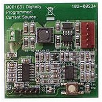
Manufacturer Part Number
MCP1631RD-MCC1
Description
REFERENCE DESIGN FOR MCP1631HV
Manufacturer
Microchip Technology
Type
Battery Managementr
Datasheets
1.MCP1631VHVT-330EST.pdf
(34 pages)
2.MCP1631HV-330EST.pdf
(54 pages)
3.MCP1631RD-MCC2.pdf
(20 pages)
4.MCP1631RD-MCC2.pdf
(328 pages)
5.MCP1631RD-MCC1.pdf
(28 pages)
Specifications of MCP1631RD-MCC1
Main Purpose
Power Management, Battery Charger
Embedded
Yes, MCU, 8-Bit
Utilized Ic / Part
MCP1631HV, PIC16F883
Primary Attributes
1 ~ 2 Cell- Li-Ion, 1 ~ 4 Cell- NiCd/NiMH
Secondary Attributes
Status LEDs
Supported Devices
MCP1631HV, PIC16F883 Device Type
Tool / Board Applications
Power Management-Battery Management
Development Tool Type
Reference Design
Input Voltage
5.5 V to 16 V
Product
Power Management Modules
Mcu Supported Families
MCP1631HV/PIC16F883 Family
Silicon Manufacturer
Microchip
Silicon Core Number
MCP1631HV
Kit Application Type
Reference Design
Application Sub Type
Battery Charger
Kit Contents
Board Only
Lead Free Status / RoHS Status
Lead free / RoHS Compliant
For Use With/related Products
MCP1631HV, PIC16F883
Lead Free Status / RoHS Status
Lead free / RoHS Compliant


3.0
The descriptions of the pins are listed in
TABLE 3-1:
3.1
Connect power ground return pin to power ground
plane, high peak current flows through the P
the turn on and turn off the external MOSFET devices.
3.2
Shutdown input logic low disables device and lowers I
to minimum value, amplifier A3 (VS) remains functional
for battery voltage sense applications.
3.3
External Oscillator Input, used to set power train
switching frequency and maximum duty cycle, V
enabled while low and disabled while high.
© 2008 Microchip Technology Inc.
TSSOP/SSOP
MCP1631/MCP1631V
8,9,10
11
12
13
14
15
16
17
18
19
20
—
—
—
1
2
3
4
5
6
7
PIN DESCRIPTIONS
Power Ground (P
Shutdown Input (SHDN)
Oscillator Input (OSC
PIN FUNCTION TABLE
2,4,12
QFN
4x4
15
16
17
18
19
20
10
11
13
14
21
—
—
1
3
5
6
7
8
9
MCP1631VHV
TSSOP/SSOP
MCP1631HV/
GND
8,9
10
11
12
13
14
15
16
17
18
19
20
—
—
1
2
3
4
5
6
7
)
IN
)
Table
GND
CS/V
A
3-1.
OSC
A
VDD_OUT
VS
OSC
COMP
SHDN
IS
P
A
P
OV
V
VDD_IN
V
MCP1631/HV/MCP1631V/VHV
Sym
VS
during
IS
NC
V
FB
EP
GND
GND
VDD
REF
EXT
OUT
OUT
IN
RAMP
IN
EXT
IN
IN
DIS
IN
Q
Power ground return
Shutdown input
External oscillator input
Oscillator disable input
Overvoltage comparator input
External voltage reference input
Quiet or analog ground
No connection
High voltage input
Analog bias voltage input
Regulated V
Voltage sense amplifier (A3) input
Current sense input
Voltage sense amplifier output
Current sense amplifier output
Error amplifier (A1) output
Error amplifier inverting input (A1)
CS - current sense input; V
Power V
External driver output
Exposed Thermal Pad (EP); must be connected to A
3.4
Oscillator disable input, used to asycnronously
terminate the V
modulate current for LED driver applications.For
minimum shutdown I
3.5
Overvoltage Comparator input, connect to voltage
divider, internal comparator terminates V
50 ns to limit output voltage to predetermined value.
3.6
External Voltage Reference input, connect fixed or
variable external reference to V
as an error amplifier, the power supply output variable
(voltage or current) will follow this input.
DD
input
DD
Oscillator Disable (OSC
Overvoltage Input (OV
External Reference Voltage Input
(V
output
REF
)
EXT
Description
Q
RAMP
duty cycle. Commonly used to
, connect OSC
voltage ramp input
REF
, with A1 configured
DS22063B-page 15
DIS
IN
DIS
)
to SHDN.
EXT
)
output in
GND
Related parts for MCP1631RD-MCC1
Image
Part Number
Description
Manufacturer
Datasheet
Request
R

Part Number:
Description:
REFERENCE DESIGN MCP1631HV
Manufacturer:
Microchip Technology
Datasheet:

Part Number:
Description:
REF DES BATT CHARG OR LED DRIVER
Manufacturer:
Microchip Technology
Datasheet:

Part Number:
Description:
Manufacturer:
Microchip Technology Inc.
Datasheet:
Part Number:
Description:
Manufacturer:
Microchip Technology Inc.
Datasheet:
Part Number:
Description:
Manufacturer:
Microchip Technology Inc.
Datasheet:
Part Number:
Description:
Manufacturer:
Microchip Technology Inc.
Datasheet:
Part Number:
Description:
Manufacturer:
Microchip Technology Inc.
Datasheet:
Part Number:
Description:
Manufacturer:
Microchip Technology Inc.
Datasheet:
Part Number:
Description:
Manufacturer:
Microchip Technology Inc.
Datasheet:
Part Number:
Description:
Manufacturer:
Microchip Technology Inc.
Datasheet: