CDB5376 Cirrus Logic Inc, CDB5376 Datasheet - Page 11
CDB5376
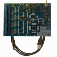
Manufacturer Part Number
CDB5376
Description
EVALUATION BOARD FOR CS5376
Manufacturer
Cirrus Logic Inc
Datasheets
1.CS5371A-ISZR.pdf
(32 pages)
2.CS4373A-ISZ.pdf
(34 pages)
3.CS5376A-IQZR.pdf
(106 pages)
4.CDB5378.pdf
(16 pages)
5.CDB5376.pdf
(80 pages)
6.CDB5376.pdf
(16 pages)
Specifications of CDB5376
Main Purpose
Seismic Evaluation System
Embedded
Yes, MCU, 8-Bit
Utilized Ic / Part
CS3301A, CS3302A, CS4373A, CS5372A, CS5376A
Primary Attributes
Quad Digital Filter
Secondary Attributes
Graphical User Interface, SPI™ & USB Interfaces
Processor To Be Evaluated
CS330x, CS4373A, CS537x
Interface Type
USB
Lead Free Status / RoHS Status
Contains lead / RoHS non-compliant
Lead Free Status / RoHS Status
Lead free / RoHS Compliant, Contains lead / RoHS non-compliant
Other names
598-1778


made using the MUX0 and MUX1 pins as shown in
Table 1 on page
Although a mux selection is provided to enable the
INA and INB switches simultaneously, signal cur-
rent should not be driven through them in this
mode. The CS3301A mux switches will maintain
good linearity only with minimal signal currents.
2.2.4
A power-down mode is available to shut down the
amplifier when not in use. When enabled, all inter-
nal circuitry is disabled, the analog inputs and out-
puts go high-impedance, and the device enters a
micro-power state. Power down mode is selected
using the PWDN pin, which is active high.
2.3
2.3.1
The analog power pins of the CS3301A are speci-
fied to run from bipolar
DS757F1
Power Supplies
Power Down Selection
Analog Power Supplies
7.
±
2.5 V power supplies.
When using bipolar power supplies, the analog sig-
nal common mode voltage should be biased to 0 V.
The analog power supplies are recommended to be
bypassed to system ground using 0.1 µF X7R type
capacitors.
The VA- supply is connected to the CMOS sub-
strate and as such must remain the most negative
applied voltage. It is recommended to clamp the
VA- supply to system ground using a reversed bi-
ased Schottky diode to prevent possible damage re-
lated to mis-matched power supply initialization.
2.3.2
The digital voltage across the VD and GND pins is
specified for a +3.3 V power supply. The digital
power supply should be bypassed to system ground
using a 0.01 µF X7R type capacitor.
Digital Power Supplies
CS3301A
11
Related parts for CDB5376
Image
Part Number
Description
Manufacturer
Datasheet
Request
R

Part Number:
Description:
Development Kit
Manufacturer:
Cirrus Logic Inc
Datasheet:
Part Number:
Description:
Development Kit
Manufacturer:
Cirrus Logic Inc
Datasheet:


Part Number:
Description:
High-efficiency PFC + Fluorescent Lamp Driver Reference Design
Manufacturer:
Cirrus Logic Inc
Datasheet:
Part Number:
Description:
Development Kit
Manufacturer:
Cirrus Logic Inc
Datasheet:
Part Number:
Description:
Development Kit
Manufacturer:
Cirrus Logic Inc
Datasheet:

Part Number:
Description:
Development Kit
Manufacturer:
Cirrus Logic Inc
Datasheet:
Part Number:
Description:
Development Kit
Manufacturer:
Cirrus Logic Inc
Datasheet:
Part Number:
Description:
Development Kit
Manufacturer:
Cirrus Logic Inc
Datasheet:
Part Number:
Description:
Development Kit
Manufacturer:
Cirrus Logic Inc
Datasheet:

Part Number:
Description:
EVALUATION BOARD FOR CS8427
Manufacturer:
Cirrus Logic Inc
Datasheet:

Part Number:
Description:
BOARD EVAL FOR CS8416 RCVR
Manufacturer:
Cirrus Logic Inc
Datasheet:

Part Number:
Description:
EVALUATION BOARD FOR CS8420
Manufacturer:
Cirrus Logic Inc
Datasheet:

Part Number:
Description:
KIT DEVELOPMENT EP9315 ARM9
Manufacturer:
Cirrus Logic Inc
Datasheet:

Part Number:
Description:
KIT DEVELOPMENT EP9302 ARM9
Manufacturer:
Cirrus Logic Inc
Datasheet: