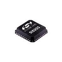
SI5325/26-EVB Silicon Laboratories Inc, SI5325/26-EVB Datasheet - Page 17

SI5325/26-EVB
Manufacturer Part Number
SI5325/26-EVB
Description
BOARD EVAL FOR SI5325/26
Manufacturer
Silicon Laboratories Inc
Specifications of SI5325/26-EVB
Main Purpose
Timing, Clock Generator
Utilized Ic / Part
SI5325, SI5326
Processor To Be Evaluated
Si5325 and Si5326
Lead Free Status / RoHS Status
Lead free / RoHS Compliant
Secondary Attributes
-
Embedded
-
Primary Attributes
-
Lead Free Status / Rohs Status
Lead free / RoHS Compliant
3. Typical Application Circuit
Note: For an example schematic and layout, refer to the Si5325/26-EVB User’s Guide.
Note: For an example schematic and layout, refer to the Si5325/26-EVB User’s Guide.
Option 1:
Option 2:
Input
Clock
Sources*
Option 1:
Option 2:
Figure 5. Si5326 Typical Application Circuit (SPI Control Mode)
Figure 4. Si5326 Typical Application Circuit (I
Control Mode (L)
Crystal/Ref Clk Rate
Input
Clock
Sources*
Control Mode (H)
Crystal/Ref Clk Rate
Crystal
Reset
Refclk+
Refclk–
Crystal
130
130
82
82
Reset
Refclk+
Refclk–
130
130
82
82
V
V
DD
DD
= 3.3 V
= 3.3 V
V
V
DD
DD
= 3.3 V
= 3.3 V
V
DD
15 k
15 k
130
130
82
82
V
0.1 µF
0.1 µF
Notes:
DD
15 k
15 k
130
130
82
82
0.1 µF
0.1 µF
Notes:
System
Supply
Power
1. Assumes differential LVPECL termination (3.3 V) on clock inputs.
2. Denotes tri-level input pins with states designated as L (ground), M (VDD/2), and H (VDD).
3. I
CKIN2+
CKIN2–
CMODE
RST
CKIN1+
CKIN1–
XA
XB
RATE[1:0]
XA
XB
System
Supply
Power
2
1. Assumes differential LVPECL termination (3.3 V) on clock inputs.
2. Denotes tri-level input pins with states designated as L (ground), M (VDD/2), and H (VDD).
C-required pull-up resistors not shown.
CKIN2+
CKIN2–
CMODE
RST
CKIN1+
CKIN1–
XA
XB
RATE[1:0]
XA
XB
2
Ferrite
Bead
2
Ferrite
Bead
Si5326
Si5326
Rev. 1.0
C
C
C
C
4
1
2
3
C
C
C
C
1 µF
0.1 µF
0.1 µF
0.1 µF
1
2
3
4
1 µF
0.1 µF
0.1 µF
0.1 µF
CKOUT1+
CKOUT1–
CKOUT2+
CKOUT2–
INT_C1B
CS_CA
CKOUT1+
CKOUT1–
CKOUT2+
CKOUT2–
A[2:0]
SDA
INT_C1B
DEC
SCL
C2B
LOL
CS_CA
INC
SCLK
SDO
DEC
C2B
LOL
SDI
INC
SS
0.1 µF
0.1 µF
0.1 µF
0.1 µF
2
0.1 µF
0.1 µF
0.1 µF
0.1 µF
100
100
Output Phase Control
C Control Mode)
Output Phase Control
100
100
Interrupt/CKIN1 Invalid Indicator
CKIN2 Invalid Indicator
PLL Loss of Lock Indicator
Serial Port Address
Serial Data
Serial Clock
Clock Select/Clock Active
Interrupt/CLKIN1 Invalid Indicator
CLKIN2 Invalid Indicator
PLL Loss of Lock Indicator
Slave Select
Serial Data Out
Serial Data In
Serial Clock
Clock Select/Clock Active
+
–
+
–
+
+
–
–
I2C Interface
Clock Outputs
SPI Interface
Clock Outputs
Si5326
17


