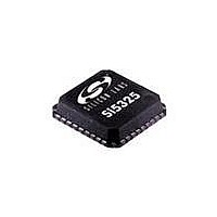
SI5325/26-EVB Silicon Laboratories Inc, SI5325/26-EVB Datasheet - Page 8

SI5325/26-EVB
Manufacturer Part Number
SI5325/26-EVB
Description
BOARD EVAL FOR SI5325/26
Manufacturer
Silicon Laboratories Inc
Specifications of SI5325/26-EVB
Main Purpose
Timing, Clock Generator
Utilized Ic / Part
SI5325, SI5326
Processor To Be Evaluated
Si5325 and Si5326
Lead Free Status / RoHS Status
Lead free / RoHS Compliant
Secondary Attributes
-
Embedded
-
Primary Attributes
-
Lead Free Status / Rohs Status
Lead free / RoHS Compliant
Si5326
8
Table 2. DC Characteristics (Continued)
(V
3-Level Input Pins
Input Voltage Low
Input Voltage Mid
Input Voltage High
Input Low Current
Input Mid Current
Input High Current
LVCMOS Output Pins
Output Voltage Low
Output Voltage Low
Output Voltage High
Output Voltage High
Disabled Leakage
Current
Notes:
DD
1.
2. No under- or overshoot is allowed.
3. LVPECL outputs require nominal V
4. This is the amount of leakage that the 3-Level inputs can tolerate from an external driver. See Si53xx
5. LVPECL, CML, LVDS and low-swing LVDS measured with Fo = 622.08 MHz.
= 1.8 ± 5%, 2.5 ±10%, or 3.3 V ±10%, T
Parameter
Current draw is independent of supply voltage
Family Reference Manual for more details.
4
Symbol
V
V
I
V
V
V
I
I
I
IMM
IHH
IMM
ILL
OZ
IHH
ILL
OH
OL
A
= –40 to 85 °C)
DD
Test Condition
≥ 2.5 V.
V
V
V
V
IO = –2 mA
See Note 4
See Note 4
See Note 4
IO = –2 mA
IO = 2 mA
DD
IO = 2 mA
DD
DD
DD
RSTb = 0
= 1.71 V
= 2.97 V
= 1.71 V
= 2.97 V
Rev. 1.0
0.45 x
0.85 x
V
V
–100
V
V
Min
–20
DD
0.4
DD
0.4
–2
—
—
—
—
DD
DD
–
–
Typ
—
—
—
—
—
—
—
—
—
—
—
0.15 x V
0.55 x V
Max
100
0.4
0.4
+2
20
—
—
—
—
DD
DD
Unit
µA
µA
µA
µA
V
V
V
V
V
V
V


