MCP3421EV Microchip Technology, MCP3421EV Datasheet - Page 3
MCP3421EV
Manufacturer Part Number
MCP3421EV
Description
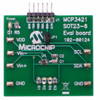
BOARD EVAL FOR MCP3421 SOT23-6
Manufacturer
Microchip Technology
Specifications of MCP3421EV
Design Resources
MCP3421EV Gerber Files
Number Of Adc's
1
Number Of Bits
18
Sampling Rate (per Second)
4
Data Interface
Serial
Inputs Per Adc
1 Single Ended
Input Range
±2.5 V
Voltage Supply Source
Single Supply
Operating Temperature
-40°C ~ 125°C
Utilized Ic / Part
MCP3421
Silicon Manufacturer
Microchip
Application Sub Type
ADC
Kit Application Type
Data Converter
Silicon Core Number
MCP3421
Kit Contents
Board
Rohs Compliant
Yes
Lead Free Status / RoHS Status
Not applicable / Not applicable
Available stocks
Company
Part Number
Manufacturer
Quantity
Price
Company:

Part Number:
MCP3421EV
Manufacturer:
Microchip Technology
Quantity:
135


1.0
1.1
V
All inputs and outputs w.r.t V
Differential Input Voltage ...................................... |V
Output Short Circuit Current ................................ Continuous
Current at Input Pins ....................................................±2 mA
Current at Output and Supply Pins ............................±10 mA
Storage Temperature ....................................-65°C to +150°C
Ambient Temp. with power applied ...............-55°C to +125°C
ESD protection on all pins ................ ≥ 6 kV HBM, ≥ 400V MM
Maximum Junction Temperature (T
1.2
ELECTRICAL CHARACTERISTICS
© 2009 Microchip Technology Inc.
Electrical Specifications: Unless otherwise specified, all parameters apply for T
V
Analog Inputs
Differential Input Range
Common-Mode Voltage Range
(absolute) (Note 1)
Differential Input Impedance
(Note 2)
Common Mode input
Impedance
System Performance
Resolution and No Missing
Codes (Note 8)
Data Rate (Note 3)
Output Noise
Integral Nonlinearity (Note 4)
Internal Reference Voltage
Note 1:
DD
IN
...................................................................................7.0V
+ = V
2:
3:
4:
5:
6:
7:
8:
IN
ELECTRICAL
CHARACTERISTICS
Absolute Maximum Ratings†
Electrical Specifications
Parameters
- = V
Any input voltage below or greater than this voltage causes leakage current through the ESD diodes at the input pins.
This parameter is ensured by characterization and not 100% tested.
This input impedance is due to 3.2 pF internal input sampling capacitor.
The total conversion speed includes auto-calibration of offset and gain.
INL is the difference between the endpoints line and the measured code at the center of the quantization band.
Includes all errors from on-board PGA and V
Full Scale Range (FSR) = 2 x 2.048/PGA = 4.096/PGA.
This parameter is ensured by characterization and not 100% tested.
This parameter is ensured by design and not 100% tested.
REF
/2. All ppm units use 2*V
SS
............... –0.3V to V
J
). .........................+150°C
Z
Z
V
Sym
IND
INC
DR
INL
REF
(f)
(f)
REF
V
as full scale range.
SS
2.75
176
Min
12
14
16
18
44
—
—
—
11
—
—
—
-0.3
DD
DD
+0.3V
- V
REF
SS
±2.048/PGA
2.25/PGA
|
.
2.048
3.75
240
Typ
1.5
25
60
15
10
—
—
—
—
—
†Notice: Stresses above those listed under “Maximum Rat-
ings” may cause permanent damage to the device. This is a
stress rating only and functional operation of the device at
those or any other conditions above those indicated in the
operational listings of this specification is not implied.
Exposure to maximum rating conditions for extended periods
may affect device reliability
V
DD
20.5
Max
328
5.1
82
35
—
—
—
—
—
—
—
—
—
+0.3
A
= -40°C to +85°C, V
ppm of
µV
Units
FSR
SPS
SPS
SPS
SPS
MΩ
MΩ
Bits
Bits
Bits
Bits
V
V
V
RMS
.
V
During normal mode operation
PGA = 1, 2, 4, 8
DR = 240 SPS
DR = 60 SPS
DR = 15 SPS
DR = 3.75 SPS
S1,S0 = ‘00’, (12 bits mode)
S1,S0 = ‘01’, (14 bits mode)
S1,S0 = ‘10’, (16 bits mode)
S1,S0 = ‘11’, (18 bits mode)
T
PGA = 1, V
DR = 3.75 SPS
(Note 6)
A
IN
= +25°C, DR = 3.75 SPS,
= V
DD
MCP3421
IN
= +5.0V, V
+ - V
IN
= 0
IN
Conditions
DS22003E-page 3
-
SS
= 0V,
Related parts for MCP3421EV
Image
Part Number
Description
Manufacturer
Datasheet
Request
R

Part Number:
Description:
Manufacturer:
Microchip Technology Inc.
Datasheet:
Part Number:
Description:
Manufacturer:
Microchip Technology Inc.
Datasheet:
Part Number:
Description:
Manufacturer:
Microchip Technology Inc.
Datasheet:
Part Number:
Description:
Manufacturer:
Microchip Technology Inc.
Datasheet:
Part Number:
Description:
Manufacturer:
Microchip Technology Inc.
Datasheet:
Part Number:
Description:
Manufacturer:
Microchip Technology Inc.
Datasheet:
Part Number:
Description:
Manufacturer:
Microchip Technology Inc.
Datasheet:
Part Number:
Description:
Manufacturer:
Microchip Technology Inc.
Datasheet: