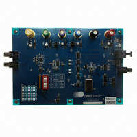
CDB5351 Cirrus Logic Inc, CDB5351 Datasheet
CDB5351
Specifications of CDB5351


Related parts for CDB5351


CDB5351 Summary of contents
Page 1
... Such applications include A/V receivers, DVD-R, CD-R, digital mixing consoles, and effects processors. ORDERING INFORMATION CS5351-KSZ, Lead Free -10° to 70°C CS5351-KZZ, Lead Free -10° to 70°C 24-pin TSSOP CS5351-DZZ, Lead Free -40° to 85°C 24-pin TSSOP CDB5351 SCLK V OVFL L Serial Output Interface ...
Page 2
TABLE OF CONTENTS 1. CHARACTERISTICS AND SPECIFICATIONS ...................................................................................... 4 SPECIFIED OPERATING CONDITIONS .............................................................................................. 4 ABSOLUTE MAXIMUM RATINGS ........................................................................................................ 4 ANALOG CHARACTERISTICS (CS5351-KSZ/KZZ) ............................................................................. 5 ANALOG CHARACTERISTICS (CS5351-DZZ) .................................................................................... 6 DIGITAL FILTER CHARACTERISTICS ................................................................................................. 7 DC ELECTRICAL CHARACTERISTICS .............................................................................................. 10 DIGITAL ...
Page 3
LIST OF FIGURES Figure 1. Single-Speed Mode Stopband Rejection ..................................................................................... 8 Figure 2. Single-Speed Mode Transition Band ........................................................................................... 8 Figure 3. Single-Speed Mode Transition Band (Detail) ............................................................................... 8 Figure 4. Single-Speed Mode Passband Ripple ......................................................................................... 8 Figure 5. Double-Speed Mode ...
Page 4
CHARACTERISTICS AND SPECIFICATIONS (All Min/Max characteristics and specifications are guaranteed over the Specified Operating Conditions. Typical performance characteristics and specifications are derived from measurements taken at typical supply voltages and T = 25°C.) A SPECIFIED OPERATING CONDITIONS (GND = ...
Page 5
ANALOG CHARACTERISTICS (CS5351-KSZ/KZZ) (Test conditions (unless otherwise specified): Input test signal kHz sine wave; measurement bandwidth kHz.) Parameter Single-Speed Mode kHz Dynamic Range Total Harmonic Distortion + Noise Double-Speed ...
Page 6
ANALOG CHARACTERISTICS (CS5351-DZZ) (Test conditions (unless otherwise specified): Input test signal kHz sine wave; measurement bandwidth kHz.) Parameter Single-Speed Mode kHz Dynamic Range Total Harmonic Distortion + Noise Double-Speed ...
Page 7
DIGITAL FILTER CHARACTERISTICS Parameter Single-Speed Mode (2 kHz to 51 kHz sample rates) Passband (-0.1 dB) Passband Ripple Stopband Stopband Attenuation Total Group Delay (Fs = Output Sample Rate) Interchannel Phase Deviation Double-Speed Mode (50 kHz to 102 kHz sample ...
Page 8
Frequency (normalized to Fs) Figure 1. Single-Speed Mode Stopband Rejection ...
Page 9
Frequency (normalized to Fs) Figure 7. Double-Speed Mode Transition Band (Detail ...
Page 10
DC ELECTRICAL CHARACTERISTICS (GND = 0 V, all voltages with respect to ground. MCLK=12.288 MHz; Master Mode) Parameter Power Supply Current (Normal Operation) Power Supply Current (Power-Down Mode) (Note 7) Power Consumption (Normal Operation VL, VD ...
Page 11
SWITCHING CHARACTERISTICS - SERIAL AUDIO PORT (Logic "0" = GND = 0 V; Logic "1" = VL, C Parameter Output Sample Rate OVFL to LRCK edge setup time OVFL to LRCK edge hold time OVFL time-out on overrange condition Fs ...
Page 12
SCLK output t mslr LRCK output t sdo SDOUT MSB Figure 13. Master Mode, Left-Justified SAI SCLK input LRCK input SDOUT Figure 15. Master Mode, I²S SAI LRCK OVFL 12 CLK input LRCK input MSB-1 SDOUT ...
Page 13
LRCK Left Channel SCLK SDATA LRCK Left Channel SCLK SDATA LRCK SCLK O VFL_R O VFL ...
Page 14
PIN DESCRIPTIONS Pin Name # Pin Description RST 1 Reset (Input) - The device enters a low power mode when low. M/S 2 Master/Slave Mode (Input) - Selects operation as either clock master or slave. 3 Left Right Clock ...
Page 15
TYPICAL CONNECTION DIAGRAM + 3 μ μ F 0.01 μF FILT μ F 0.01 μF REFGND AINL Analog VQ1 Input Buffer VQ3 (Figure 24) VQ2 AINR DS565F2 + 0.01 ...
Page 16
APPLICATIONS 4.1 Operational Mode/Sample Rate Range Select The output sample rate, Fs, can be adjusted from 2 kHz to 204 kHz. The CS5351 must be set to the proper speed mode via the mode pins, M1 and M0. Refer ...
Page 17
Master Mode In Master Mode, LRCK and SCLK operate as outputs. The left/right and serial clocks are internally derived from the master clock with the left/right clock equal to Fs and the serial clock equal to 64x Fs, as ...
Page 18
Analog Connections The analog modulator samples the input at 6.144 MHz. The digital filter will reject signals within the stop- band of the filter. However, there is no rejection for input signals which are (n band frequency, where n=0,1,2,...Refer ...
Page 19
... FILT+ and VQ pins in order to avoid unwanted coupling into the modulators. The FILT+ and VQ decoupling capacitors, particularly the 0.01 µF, must be positioned to minimize the electrical path from FILT+ and REFGND. The CDB5351 evaluation board demonstrates the optimum layout and power supply arrangements. To minimize digital noise, connect the ADC digital outputs only to CMOS inputs. ...
Page 20
PARAMETER DEFINITIONS Dynamic Range The ratio of the rms value of the signal to the rms sum of all other spectral components over the specified bandwidth. Dynamic Range is a signal-to-noise ratio measurement over the specified bandwidth made with ...
Page 21
PACKAGE DIMENSIONS 24L SOIC (300 MIL BODY) PACKAGE DRAWING 1 b SEATING PLANE e DIM ∝ DS565F2 E D INCHES MIN MAX MIN 0.093 0.104 2.35 0.004 0.012 0.10 0.013 ...
Page 22
TSSOP (4.4 mm BODY) PACKAGE DRAWING TOP VIEW INCHES DIM MIN NOM 0.002 0.004 A2 0.03346 0.0354 b 0.00748 0.0096 D 0.303 0.307 E 0.248 0.2519 E1 0.169 0.1732 e -- ...
Page 23
REVISION HISTORY Release PP2 Preliminary datasheet. F1 Improve Gain Error specification under Analog Characteristics. Specify Full-scale Input Voltage in terms of VA under Analog Characteristics. Update Differential Input Impedance under Analog Characteristics. Increase maximum Power-Supply Current, I Reduce maximum ...