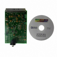
EVAL-AD7767-1EDZ Analog Devices Inc, EVAL-AD7767-1EDZ Datasheet
EVAL-AD7767-1EDZ
Specifications of EVAL-AD7767-1EDZ


Related parts for EVAL-AD7767-1EDZ


EVAL-AD7767-1EDZ Summary of contents
Page 1
FEATURES Oversampled successive approximation (SAR) architecture High performance ac and dc accuracy, low power 115.5 dB dynamic range, 32 kSPS (AD7767-2) 112.5 dB dynamic range, 64 kSPS (AD7767-1) 109.5 dB dynamic range, 128 kSPS (AD7767) −118 dB THD Exceptionally low ...
Page 2
AD7767 TABLE OF CONTENTS Features .............................................................................................. 1 Applications ....................................................................................... 1 Functional Block Diagram .............................................................. 1 General Description ......................................................................... 1 Related Devices ................................................................................. 1 Revision History ............................................................................... 2 Specifications ..................................................................................... 3 Timing Specifications .................................................................. 5 Timing Diagrams .......................................................................... 6 Absolute Maximum ...
Page 3
SPECIFICATIONS 2.5 V ± DRIVE unless otherwise noted. Table 2. Parameter OUTPUT DATA RATE (ODR) AD7767 AD7767-1 AD7767-2 1 ANALOG INPUT Differential Input Voltage Absolute ...
Page 4
AD7767 Parameter 1 DIGITAL FILTER RESPONSE Group Delay Settling Time (Latency) Pass-Band Ripple Pass Band −3 dB Bandwidth Stop-Band Frequency Stop-Band Attenuation REFERENCE INPUT 1 V Input Voltage REF+ 1 DIGITAL INPUTS (Logic Levels Input Leakage ...
Page 5
TIMING SPECIFICATIONS 2.5 V ± DRIVE 1 unless otherwise noted. Table 3. Parameter Limit at t DRDY OPERATION t 510 100 2 ...
Page 6
AD7767 TIMING DIAGRAMS 1 MCLK t 1 DRDY Figure 2. DRDY vs. MCLK Timing Diagram for AD7767 (Decimate by 8 for AD7767-1 (Decimate by 16 for AD7767-2 (Decimate by 32) DRDY ...
Page 7
PART IN POWER-DOWN MCLK ( SYNC/PD ( DRDY (O) VALID DATA DOUT (O) Figure 5. Reset, Synchronization, and Power-Down Timing (For More Information, See the Power-Down, Reset, and Synchronization Section) PART OUT OF POWER-DOWN FILTER ...
Page 8
AD7767 ABSOLUTE MAXIMUM RATINGS T = 25°C, unless otherwise noted. A Table 4. Parameter AV to AGND DGND REFGND REF+ REFGND to AGND V to DGND DRIVE V , ...
Page 9
PIN CONFIGURATION AND FUNCTION DESCRIPTIONS Table 5. Pin Function Descriptions Pin No. Mnemonic Description 1 AV +2.5 V Analog Power Supply Reference Input for the AD7767. An external reference must be applied to this input pin. The ...
Page 10
AD7767 TYPICAL PERFORMANCE CHARACTERISTICS 2.5 V ± DRIVE otherwise noted. All FFTs were generated using 8192 samples using a four-term Blackman-Harris window. 0 –20 –40 ...
Page 11
FREQUENCY (Hz) Figure 13. AD7767 FFT, 1 kHz, −60 dB Input Tone 0 –20 –40 –60 –80 –100 –120 –140 –160 –180 0 ...
Page 12
AD7767 –110 –112 –114 –116 AD7767-2 –118 –120 –122 AD7767-1 AD7767 –124 –126 –128 –130 0 100k 200k 300k 400k 500k 600k MCLK FREQUENCY (Hz) Figure 19. AD7767/AD7767-1/AD7767-2 THD vs. MCLK Frequency 115 114 AD7767-2 113 112 111 AD7767-1 110 ...
Page 13
MAX = 8388593 350 MIN = 8388526 SPREAD = 69 CODES 300 250 200 150 100 50 0 CODES Figure 25. AD7767-2 24-Bit Histogram 1.0 0.8 0.6 0.4 0.2 0 –0.2 –0.4 –0.6 –0.8 –1.0 0 4194304 8388608 12582912 2097152 ...
Page 14
AD7767 TERMINOLOGY Signal-to-Noise Ratio (SNR) SNR is the ratio of the actual input signal’s rms value to the rms sum of all other spectral components below the Nyquist frequency, excluding harmonics and dc. The value for SNR is expressed in ...
Page 15
THEORY OF OPERATION The AD7767/AD7767-1/AD7767-2 operate using a fully differential analog input applied to a successive approximation (SAR) core. The output of the oversampled SAR is filtered using a linear-phase digital FIR filter. The fully filtered data is output in ...
Page 16
AD7767 0 –20 –40 –60 –80 –100 –120 –140 –160 0 16k 32k 48k 64k 80k FREQUENCY (Hz) Figure 32. AD7767 Digital Filter Frequency Response 0 –20 –40 –60 –80 –100 –120 –140 –160 0 8k 16k 24k 32k 40k ...
Page 17
AD7767 INTERFACE The AD7767 provides the user with a flexible serial interface, enabling the user to implement the most desirable interfacing scheme for their application. The AD7767 interface comprises seven different signals. Five of these signals are inputs: MCLK, CS ...
Page 18
AD7767 DAISY CHAINING Daisy chaining devices allows numerous devices to use the same digital interface lines by cascading the outputs of multiple ADCs on a single data line. This feature is especially useful for reduc- ing component count and wiring ...
Page 19
DAISY-CHAIN MODE CONFIGURATION AND TIMING DIAGRAMS SYNC/PD CS SYNC/PD CS AD7767 (D) SDI SDI SCLK MCLK SCLK MCLK 1 MCLK DRDY ( × SCLK SCLK AD7767 (A) SDO (A) SDI (A) = SDO (B) AD7767 (B) AD7767 ...
Page 20
AD7767 DRIVING THE AD7767 The AD7767 must be driven with fully differential inputs. The common-mode voltage of the differential inputs to the AD7767 device and therefore the limits on the differential inputs are set by the reference voltage (V ) ...
Page 21
ANTIALIASING The AD7767/AD7767-1/AD7767-2 sample the analog input at a maximum rate of 1.024 MHz. The on-board digital filter provides up to 100 dB attenuation for any possible aliasing frequency in the range from the beginning of the filter stop band ...
Page 22
AD7767 V INPUT SIGNAL REF+ The AD7767/AD7767-1/AD7767-2 V REF + voltage in the range of 2 × recommended that the V input be generated by a low noise REF+ voltage reference. Examples of such references ...
Page 23
... AD7767BRUZ-RL7 −40°C to +105°C AD7767BRUZ-1 −40°C to +105°C AD7767BRUZ-1-RL7 −40°C to +105°C AD7767BRUZ-2 −40°C to +105°C AD7767BRUZ-2-RL7 −40°C to +105°C EVAL-AD7767EDZ EVAL-AD7767-1EDZ EVAL-AD7767-2EDZ EVAL-CED1Z RoHS Compliant Part. 5.10 5.00 4. 4.50 6.40 4.40 BSC 4 ...
Page 24
AD7767 NOTES ©2007–2010 Analog Devices, Inc. All rights reserved. Trademarks and registered trademarks are the property of their respective owners. D06859-0-5/10(C) Rev Page ...