EVAL-AD7767-1EDZ Analog Devices Inc, EVAL-AD7767-1EDZ Datasheet - Page 14
EVAL-AD7767-1EDZ
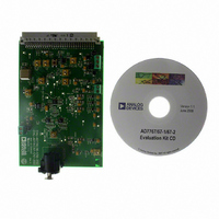
Manufacturer Part Number
EVAL-AD7767-1EDZ
Description
BOARD EVAL AD7767-1 64KSPS 111DB
Manufacturer
Analog Devices Inc
Specifications of EVAL-AD7767-1EDZ
Number Of Adc's
1
Number Of Bits
24
Sampling Rate (per Second)
64k
Data Interface
Serial
Inputs Per Adc
1 Differential
Input Range
±VREF
Power (typ) @ Conditions
10.5mW @ 64kSPS
Voltage Supply Source
Analog and Digital
Operating Temperature
-40°C ~ 105°C
Utilized Ic / Part
AD7767-1
Lead Free Status / RoHS Status
Lead free / RoHS Compliant


AD7767
TERMINOLOGY
Signal-to-Noise Ratio (SNR)
SNR is the ratio of the actual input signal’s rms value to the rms
sum of all other spectral components below the Nyquist frequency,
excluding harmonics and dc. The value for SNR is expressed in
decibels.
Total Harmonic Distortion (THD)
THD is the ratio of the rms sum of harmonics to the fundamen-
tal. For the AD7767, it is defined as
where:
V
V
the sixth harmonics.
Nonharmonic Spurious-Free Dynamic Range (SFDR)
SFDR is the ratio of the rms signal amplitude to the rms value
of the peak spurious spectral component, excluding harmonics.
Dynamic Range
Dynamic range is the ratio of the rms value of the full scale to
the rms noise measured with the inputs shorted together. The
value for the dynamic range is expressed in decibels.
Intermodulation Distortion (IMD)
With inputs consisting of sine waves at two frequencies, fa
and fb, any active device with nonlinearities creates distortion
products at sum and difference frequencies of mfa ± nfb, where
m, n = 0, 1, 2, 3, and so on. Intermodulation distortion terms
are those for which neither m nor n are equal to 0. For example,
the second-order terms include (fa + fb) and (fa − fb), and the
third-order terms include (2fa + fb), (2fa − fb), (fa + 2fb), and
(fa − 2fb).
The AD7767 is tested using the CCIF standard, where two input
frequencies near the top end of the input bandwidth are used.
In this case, the second-order terms are usually distanced in
frequency from the original sine waves, and the third-order
terms are usually at a frequency close to the input frequencies.
As a result, the second- and third-order terms are specified
separately. The calculation of the intermodulation distortion is
1
2
, V
is the rms amplitude of the fundamental.
THD
3
, V
4
, V
( )
dB
5
, and V
=
20
6
log
are the rms amplitudes of the second to
V
2
2
+
V
3
2
+
V
V
1
4
2
+
V
5
2
+
V
6
2
Rev. C | Page 14 of 24
as per the THD specification, where it is the ratio of the rms
sum of the individual distortion products to the rms amplitude
of the sum of the fundamentals expressed in decibels.
Integral Nonlinearity (INL)
INL is the maximum deviation from a straight line passing
through the endpoints of the ADC transfer function.
Differential Nonlinearity (DNL)
DNL is the difference between the measured and the ideal
1 LSB change between any two adjacent codes in the ADC.
Zero Error
Zero error is the difference between the ideal midscale input
voltage (when both inputs are shorted together) and the actual
voltage producing the midscale output code.
Zero Error Drift
Zero error drift is the change in the actual zero error value due
to a temperature change of 1°C. It is expressed as a percentage
of full scale at room temperature.
Gain Error
The first transition (from 100 … 000 to 100 … 001) should occur
½ LSB above the nominal negative full scale for an analog voltage.
The last transition (from 011 … 110 to 011 … 111) should occur
1½ LSB below the nominal full scale for an analog voltage. The
gain error is the deviation of the difference between the actual
level of the last transition and the actual level of the first transition,
from the difference between the ideal levels.
Gain Error Drift
Gain error drift is the change in the actual gain error value due
to a temperature change of 1°C. It is expressed as a percentage
of full scale at room temperature.
Common-Mode Rejection Ratio (CMRR)
CMRR is defined as the ratio of the power in the ADC output
at full-scale frequency f to the power of a 100 mV sine wave
applied to the common-mode voltage of the V
inputs at frequency f
where Pf is the power at the frequency f in the ADC output, and
Pf
S
is the power at the frequency f
CMRR (dB) = 10 log( Pf / Pf
S
.
S
)
S
in the ADC output.
IN+
and V
IN−
Related parts for EVAL-AD7767-1EDZ
Image
Part Number
Description
Manufacturer
Datasheet
Request
R

Part Number:
Description:
IC, ADJ LDO REG, 1.5V TO 5V 250mA MSOP-8
Manufacturer:
Vishay
Datasheet:

Part Number:
Description:
IC, ADJ LDO REG, 1.5V TO 5V 0.6A 8-TSSOP
Manufacturer:
Vishay
Datasheet:
Part Number:
Description:
IC, ADJ LDO REG, 1.5V TO 5V 250mA MSOP-8
Manufacturer:
Vishay
Datasheet:

Part Number:
Description:
IC ADJ LDO REG 1.5V TO 5V 150mA 5-SOT-23
Manufacturer:
Vishay
Datasheet:

Part Number:
Description:
BOARD EVAL AS1324-AD
Manufacturer:
austriamicrosystems
Datasheet:
Part Number:
Description:
IC, ADJ LDO REG, 1.5V TO 5V 0.6A 8-TSSOP
Manufacturer:
Vishay
Datasheet:

Part Number:
Description:
IC, ADJ LDO REG, 1.5V TO 5V, 0.3A, MSOP8
Manufacturer:
Vishay
Datasheet:
Part Number:
Description:
IC, ADJ LDO REG, 1.5V TO 5V, 0.3A, MSOP8
Manufacturer:
Vishay
Datasheet:
Part Number:
Description:
IC, ADJ LDO REG 1.215V TO 5V 0.3A MSOP-8
Manufacturer:
Vishay
Datasheet:
Part Number:
Description:
IC, ADJ LDO REG 1.215V TO 5V 0.3A MSOP-8
Manufacturer:
Vishay
Datasheet:

Part Number:
Description:
±1.7g Dual-Axis IMEMS Accelerometer Evaluation Board
Manufacturer:
Analog Devices Inc
Datasheet:

Part Number:
Description:
IC MULTIPLIER ANALOG 8-SOIC T/R
Manufacturer:
Analog Devices Inc
Datasheet:

Part Number:
Description:
IC ANALOG MULTIPLIER 8-DIP
Manufacturer:
Analog Devices Inc
Datasheet:
Part Number:
Description:
IC ANALOG MULTIPLIER 8-SOIC
Manufacturer:
Analog Devices Inc
Datasheet:
Part Number:
Description:
IC ANALOG MULTIPLIER 8-DIP
Manufacturer:
Analog Devices Inc
Datasheet: