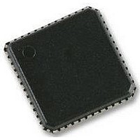
AD9246-125EBZ Analog Devices Inc, AD9246-125EBZ Datasheet - Page 25

AD9246-125EBZ
Manufacturer Part Number
AD9246-125EBZ
Description
BOARD EVAL FOR 125MSPS AD9246
Manufacturer
Analog Devices Inc
Datasheet
1.AD9246BCPZ-125.pdf
(44 pages)
Specifications of AD9246-125EBZ
Design Resources
Using AD8376 to Drive Wide Bandwidth ADCs for High IF AC-Coupled Appls (CN0002) Driving AD9233/46/54 ADCs in AC-Coupled Baseband Appls (CN0051)
Number Of Adc's
1
Number Of Bits
14
Sampling Rate (per Second)
125M
Data Interface
Serial
Inputs Per Adc
1 Differential
Input Range
2 Vpp
Power (typ) @ Conditions
458mW @ 125MSPS
Voltage Supply Source
Single Supply
Operating Temperature
-40°C ~ 85°C
Utilized Ic / Part
AD9246-125
Silicon Manufacturer
Analog Devices
Application Sub Type
ADC
Kit Application Type
Data Converter
Silicon Core Number
AD9246
Kit Contents
Board
Power Dissipation Pd
458mW
Input Channels Per Adc
1
Lead Free Status / RoHS Status
Lead free / RoHS Compliant
MEMORY MAP REGISTER TABLE
Table 15. Memory Map Register
Addr.
(Hex)
Chip Configuration Registers
00
01
02
Device Index and Transfer Registers
FF
Global ADC Functions
08
09
Parameter Name
chip_port_config
chip_id
chip_grade
device_update
modes
clock
Bit 7
(MSB)
0
Open
Open
Open
Open
Bit 6
LSB first
0 = Off
(Default)
1 = On
Open
Open
Open
Open
Bit 5
Soft reset
0 = Off
(Default)
1 = On
Open
Open
PDWN
0—full
(Default)
1—standby
Open
(AD9246 = 0x00), (default)
Bit 4
1
Open
Open
Open
Open
8-bit Chip ID Bits 7:0
Rev. A | Page 25 of 44
Bit 3
1
Child ID
0 = 125
MSPS,
1 = 105
MSPS
Open
Open
Open
Soft reset
0 = Off
(Default)
1 = On
Bit 2
Open
Open
Internal power-down mode
000—normal (power-up, Default)
001—full power-down
010—standby
011—normal (power-up)
Note: External PDWN pin overrides
this setting.
Open
Open
Bit 1
LSB first
0 = Off
(Default)
1 = On
Open
Open
Duty cycle
stabilizer
0—disabled
1— enabled
(Default)
SW transfer
Bit 0
(LSB)
0
Open
Default
Value
(Hex)
0x18
Read
only
Read
only
0x00
0x00
0x01
Default Notes/
Comments
The nibbles
should be
mirrored. See the
Interfacing to
High Speed ADCs
via SPI User
Manual
Default is unique
chip ID, different
for each device.
Child ID used to
differentiate
speed grades.
Synchronously
transfers data
from the master
shift register to
the slave.
Determines
various generic
modes of chip
operation. See
the
Dissipation
and Standby
Mode
and the
Accessible
Features
section.
See the
Duty Cycle
section and the
SPI-Accessible
Features
section.
AD9246
Power
.
section
Clock
SPI-


