CDB35L00 Cirrus Logic Inc, CDB35L00 Datasheet
CDB35L00
Specifications of CDB35L00


Related parts for CDB35L00


CDB35L00 Summary of contents
Page 1
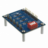
... Component landings are available for an optional EMI output filter. The CDB35L00-X4 can be configured to evaluate the four operational modes and two gain settings of the CS35L00 amplifier. Mode, Gain, and Shutdown control is available through the S1 switch. Hybrid control is available through the R13, R23, R33, and R43 resistors ...
Page 2
... Figure 2.Shutdown Control Resistors ......................................................................................................... 5 Figure 3.Optional Bypass Trace Cut Locations for U1 ................................................................................ 6 Figure 4.CDB35L00-X4 Schematic ............................................................................................................. 9 Figure 5.CDB35L00-X4 Top Side Component Placement ........................................................................ 11 Figure 6.CDB35L00-X4 Bottom Side Component Placement ................................................................... 11 Figure 7.CDB35L00-X4 Layer 1 Copper ................................................................................................... 11 Figure 8.CDB35L00-X4 Layer 2 Copper ................................................................................................... 11 Figure 9.CDB35L00-X4 Layer 3 Copper ................................................................................................... 11 Figure 10.CDB35L00-X4 Layer 4 Copper ................................................................................................. 11 LIST OF TABLES Table 1. S1 Switch GAIN & ...
Page 3
... Power Supply A single +2.5 to +5.5 VDC power supply is required to power the CDB35L00-X4. The supply must be capa- ble of delivering sufficient current for the intended power output. The supply provides power to each of the four CS35L00 amplifiers. The power supply connection to the board is provided by the header J1. The pos- itive terminal is labeled VBATT ...
Page 4
... Table 2. Hybrid Control Resistor & S1 Switch MODE Configurations 1.4 Shutdown Control The S1 switch implements shutdown control for the four CS35L00 devices on the CDB35L00-X4. SD1-2 controls the shutdown for U1 and U2. SD3-4 controls the shutdown for U3 and U4 as shown in on the schematic in Figure 4 on page ...
Page 5
... Optional Gain Adjustment Resistors The CDB35L00-X4 contains optional gain adjustment resistor placeholders for each CS35L00 device (R11, R12, R21, R22, R31, R32, R41, R42). By default these are not populated and the CS35L00 oper- ates at its gain control setting as set by the S1 switch. See necessary when a gain gain of + not desired ...
Page 6
... Optional Speaker Output EMI Filter Components The CDB35L00-X4 contains optional placeholders for a series ferrite bead (FB11, FB12, FB21, FB22, FB31, FB32, FB41, FB42) and shunt capacitor (C16, C17, C26, C27, C36, C37, C46, C47) output filter. For most applications with very short speaker leads between the CS35L00 and the speaker, use of these components will not be necessary ...
Page 7
... The small value decoupling capacitors are placed as close as possible to the power pins of the CS35L00 on the CDB35L00-X4 board recommended that the power supply decoupling capacitors reside on the opposite side of the board from which the CS35L00 is populated on. This allows for very close placement of the decoupling capacitors to the power supply pins of the CS35L00 without interfering with the differential audio inputs or differential audio outputs ...
Page 8
... Low = CS35L00 frequency reduced operational mode (FSD or FHD) High = CS35L00 non-frequency reduced operational mode (SD or HD) Low = CS35L00 shutdown enabled High = CS35L00 shutdown disabled Low = CS35L00 shutdown enabled High = CS35L00 shutdown disabled Table 5. S1 Switch Settings CDB35L00-X4 Connector Function Function Selected DS913DB2 ...
Page 9
... CDB SCHEMATIC DS913DB2 Figure 4. CDB35L00-X4 Schematic CDB35L00-X4 9 ...
Page 10
... Bill of Materials The component listing below is shown for the CDB35L00-X4 board. Unpopulated (DNP) components are listed with recommended components for reference purposes. Qty Reference Designator( C11, C12, C21, C22, C31, C32, C41, C42 4 C13, C23, C33, C43 4 C15, C25, C35, C45 ...
Page 11
... CDB LAYOUT Figure 5. CDB35L00-X4 Top Side Component Placement Figure 8. CDB35L00-X4 Layer 2 Copper DS913DB2 Figure 6. CDB35L00-X4 Bottom Side Component Placement Figure 9. CDB35L00-X4 Layer 3 Copper CDB35L00-X4 Figure 7. CDB35L00-X4 Layer 1 Copper Figure 10. CDB35L00-X4 Layer 4 Copper 11 ...
Page 12
... Updated Figure 4 on page 9 – Updated BOM values for C6 & the typical connection diagram in the DS906A2 device datasheet. All CDB35L00-X4 boards with an assembly date of 02/15/10 or earlier contain components from the Rev A0 BOM. Contacting Cirrus Logic Support For all product questions and inquiries, contact a Cirrus Logic Sales Representative. ...