EVL6566B-40WSTB STMicroelectronics, EVL6566B-40WSTB Datasheet - Page 24
EVL6566B-40WSTB
Manufacturer Part Number
EVL6566B-40WSTB
Description
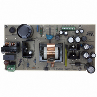
BOARD EVAL FOR L6566B
Manufacturer
STMicroelectronics
Datasheet
1.L6566BTR.pdf
(51 pages)
Specifications of EVL6566B-40WSTB
Main Purpose
AC/DC, Primary Side
Outputs And Type
4, Isolated
Power - Output
40W
Voltage - Output
5V, 12V, 1.8V, 3.3V
Current - Output
2.4A, 1.9A, 1.73A, 500mA
Voltage - Input
90 ~ 264VAC
Regulator Topology
Flyback
Frequency - Switching
62kHz
Board Type
Fully Populated
Utilized Ic / Part
L6566B
Product
Power Management Modules
Lead Free Status / RoHS Status
Lead free / RoHS Compliant
Other names
497-6450
Available stocks
Company
Part Number
Manufacturer
Quantity
Price


Application information
5.3
Note:
24/51
Burst-mode operation at no load or very light load
When the voltage at the COMP pin (9) falls 20 mV below a threshold fixed internally at a
value, V
the MOSFET kept in OFF state and its consumption reduced at a lower value to minimize
Vcc capacitor discharge.
The control voltage now will increase as a result of the feedback reaction to the energy
delivery stop (the output voltage will be slowly decaying), the threshold will be exceeded and
the device will restart switching again. In this way the converter will work in burst-mode with
a nearly constant peak current defined by the internal disable level. A load decrease will
then cause a frequency reduction, which can go down even to few hundred hertz, thus
minimizing all frequency-related losses and making it easier to comply with energy saving
regulations. This kind of operation, shown in the timing diagrams of
others previously described, is noise-free since the peak current is low.
If it is necessary to decrease the intervention threshold of the burst-mode operation, this can
be done by adding a small DC offset on the current sense pin as shown in
page 25
The offset reduces the available dynamics of the current signal; thereby, the value of the
sense resistor must be determined taking this offset into account.
Figure 11. Load-dependent operating modes: timing diagrams
MODE/SC=Open
MODE/SC=VREF
(pin 4)
COMPBM
COMP
(pin 9)
.
V
COMPBM
GD
f
f
sw
osc
, depending on the selected operating mode, the L6566B is disabled with
QR Mode
FF Mode
Valley-skipping Mode
Burst-mode
Burst-mode
Figure 11
FF Mode
Figure 12 on
MODE/SC=Open
MODE/SC=VREF
along with the
QR Mode
hyster.
20 mV
L6566B
t
t
t
Related parts for EVL6566B-40WSTB
Image
Part Number
Description
Manufacturer
Datasheet
Request
R

Part Number:
Description:
BOARD EVAL SMPS FOR L6566B
Manufacturer:
STMicroelectronics
Datasheet:

Part Number:
Description:
BOARD EVAL FOR L6566B
Manufacturer:
STMicroelectronics
Datasheet:

Part Number:
Description:
BOARD EVAL FOR L6566B
Manufacturer:
STMicroelectronics
Datasheet:

Part Number:
Description:
Power Management Modules & Development Tools L6566B-60WQR Eval Board
Manufacturer:
STMicroelectronics
Part Number:
Description:
STMicroelectronics [RIPPLE-CARRY BINARY COUNTER/DIVIDERS]
Manufacturer:
STMicroelectronics
Datasheet:
Part Number:
Description:
STMicroelectronics [LIQUID-CRYSTAL DISPLAY DRIVERS]
Manufacturer:
STMicroelectronics
Datasheet:

Part Number:
Description:
BOARD EVAL FOR MEMS SENSORS
Manufacturer:
STMicroelectronics
Datasheet:
Part Number:
Description:
NPN TRANSISTOR POWER MODULE
Manufacturer:
STMicroelectronics
Datasheet:
Part Number:
Description:
TURBOSWITCH ULTRA-FAST HIGH VOLTAGE DIODE
Manufacturer:
STMicroelectronics
Datasheet:
Part Number:
Description:
Manufacturer:
STMicroelectronics
Datasheet:
Part Number:
Description:
DIODE / SCR MODULE
Manufacturer:
STMicroelectronics
Datasheet:
Part Number:
Description:
DIODE / SCR MODULE
Manufacturer:
STMicroelectronics
Datasheet: