AD9785-EBZ Analog Devices Inc, AD9785-EBZ Datasheet - Page 23
AD9785-EBZ
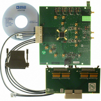
Manufacturer Part Number
AD9785-EBZ
Description
BOARD EVAL FOR AD9785
Manufacturer
Analog Devices Inc
Series
TxDAC®r
Datasheet
1.AD9785BSVZ.pdf
(64 pages)
Specifications of AD9785-EBZ
Number Of Dac's
2
Number Of Bits
12
Outputs And Type
2, Differential
Sampling Rate (per Second)
800M
Data Interface
Serial
Settling Time
22ms
Dac Type
Current
Voltage Supply Source
Analog and Digital
Operating Temperature
-40°C ~ 85°C
Utilized Ic / Part
AD9785
Silicon Manufacturer
Analog Devices
Application Sub Type
DAC
Kit Application Type
Data Converter
Silicon Core Number
AD9785
Kit Contents
Board
Lead Free Status / RoHS Status
Lead free / RoHS Compliant
Lead Free Status / RoHS Status
Lead free / RoHS Compliant, Lead free / RoHS Compliant


Instruction Byte
The instruction byte contains the following information as
shown in the instruction byte bit map.
Instruction Byte Information Bit Map
MSB
D7
R/W
R/ W —Bit 7 of the instruction byte determines whether a read
or write data transfer occurs after the instruction byte write.
Logic 1 indicates a read operation. Logic 0 indicates a write
operation.
X, X —Bit 6 and Bit 5 of the instruction byte are don’t care. In
previous TxDACs, such as the AD9779, these bits define the
number of registers written to or read from in an SPI read/write
operation. In the AD9785/AD9787/AD9788, the register itself
now defines how many bytes are written to or read from.
A4, A3, A2, A1, A0—Bit 4, Bit 3, Bit 2, Bit 1, and Bit 0 of the
instruction byte determine which register is accessed during the
data transfer portion of the communication cycle.
Serial Interface Port Pin Description
SCLK—Serial Clock
The serial clock pin is used to synchronize data to and from the
AD9785/AD9787/AD9788 and to run the internal state machines.
SCLK maximum frequency is 40 MHz.
SPI_CSB—Chip Select
Active low input that allows more than one device on the same
serial communications line. The SPI_SDO and SPI_SDIO pins
go to a high impedance state when this input is high. If driven
high during any communication cycle, that cycle is suspended
until SPI_CSB is reactivated low. Chip select can be tied low in
systems that maintain control of SCLK.
SPI_SDIO—Serial Data I/O
Data is always written into the AD9785/AD9787/AD9788 on
this pin. However, this pin can be used as a bidirectional data
line. Bit 7 of Register 0x00 controls the configuration of this pin.
The default is Logic 0, which configures the SPI_SDIO pin for
input only (4-wire) operation.
D6
X
D5
X
D4
A4
D3
A3
D2
A2
D1
A1
LSB
D0
A0
Rev. A | Page 23 of 64
SPI_SDO—Serial Data Output
Data is read from this pin for protocols that use separate lines
for transmitting and receiving data. In the case where the
AD9785/AD9787/AD9788 operate in a single bidirectional
I/O mode, this pin does not output data and is set to a high
impedance state.
MSB/LSB Transfers
The AD9785/AD9787/AD9788 serial port can support both
most significant bit (MSB) first or least significant bit (LSB)
first data formats. This functionality is controlled by Bit 6 of the
communication (COMM) register. The default value of COMM
Register Bit 6 is low (MSB first). When COMM Register Bit 6 is
set high, the serial port is in LSB first format. The instruction byte
must be written in the format indicated by COMM Register Bit 6.
That is, if the device is in LSB first mode, the instruction byte
must be written from least significant bit to most significant bit.
For MSB first operation, the serial port controller generates the
most significant byte (of the specified register) address first,
followed by the next lesser significant byte addresses until the
I/O operation is complete. All data written to or read from the
AD9785/AD9787/AD9788 must be in MSB first order.
If the LSB mode is active, the serial port controller generates the
least significant byte address first, followed by the next greater
significant byte addresses until the I/O operation is complete.
All data written to or read from the AD9785/AD9787/AD9788
must be in LSB first order.
SPI Resynchronization Capability
If the SPI port becomes unsynchronized at any time, toggling
SCLK for eight or more cycles with SPI_CSB held high resets
the SPI port state machine. The device is then ready for the next
register read or write access.
AD9785/AD9787/AD9788
Related parts for AD9785-EBZ
Image
Part Number
Description
Manufacturer
Datasheet
Request
R

Part Number:
Description:
Dual 16B, 1.0 GSPS TxDAC
Manufacturer:
Analog Devices Inc
Datasheet:

Part Number:
Description:
±1.7g Dual-Axis IMEMS Accelerometer Evaluation Board
Manufacturer:
Analog Devices Inc
Datasheet:
Part Number:
Description:
Inertial Sensor Evaluation System
Manufacturer:
Analog Devices Inc
Datasheet:
Part Number:
Description:
Manufacturer:
Analog Devices Inc
Datasheet:
Part Number:
Description:
Manufacturer:
Analog Devices Inc
Datasheet:
Part Number:
Description:
Manufacturer:
Analog Devices Inc
Datasheet:
Part Number:
Description:
Manufacturer:
Analog Devices Inc
Datasheet:
Part Number:
Description:
Manufacturer:
Analog Devices Inc
Datasheet:
Part Number:
Description:
Manufacturer:
Analog Devices Inc
Datasheet:
Part Number:
Description:
Manufacturer:
Analog Devices Inc
Datasheet:
Part Number:
Description:
Manufacturer:
Analog Devices Inc
Datasheet:
Part Number:
Description:
Manufacturer:
Analog Devices Inc
Datasheet:
Part Number:
Description:
Manufacturer:
Analog Devices Inc
Datasheet: