AD9785-EBZ Analog Devices Inc, AD9785-EBZ Datasheet - Page 40
AD9785-EBZ
Manufacturer Part Number
AD9785-EBZ
Description
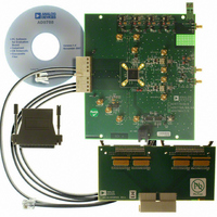
BOARD EVAL FOR AD9785
Manufacturer
Analog Devices Inc
Series
TxDAC®r
Datasheet
1.AD9785BSVZ.pdf
(64 pages)
Specifications of AD9785-EBZ
Number Of Dac's
2
Number Of Bits
12
Outputs And Type
2, Differential
Sampling Rate (per Second)
800M
Data Interface
Serial
Settling Time
22ms
Dac Type
Current
Voltage Supply Source
Analog and Digital
Operating Temperature
-40°C ~ 85°C
Utilized Ic / Part
AD9785
Silicon Manufacturer
Analog Devices
Application Sub Type
DAC
Kit Application Type
Data Converter
Silicon Core Number
AD9785
Kit Contents
Board
Lead Free Status / RoHS Status
Lead free / RoHS Compliant
Lead Free Status / RoHS Status
Lead free / RoHS Compliant, Lead free / RoHS Compliant


AD9785/AD9787/AD9788
QUADRATURE MODULATOR
The quadrature modulator is used to mix the carrier signal
generated by the NCO with the upsampled I and Q data
provided by the user at the 16-bit parallel input port of the
device. Figure 58 shows a detailed block diagram of the
quadrature modulator.
The NCO provides a quadrature carrier signal with a frequency
determined by the 32-bit frequency tuning word (FTW) set in
Register 0x0A, Bits [31:0]. The NCO operates at the rate equal
to the upsampled I data and Q data. The generated carrier
signal is mixed via multipliers with the I data and Q data. The
quadrature products are then summed.
Note that the sine output of the NCO contains a mux that
allows negating of the data. The mux is controlled with a
spectral inversion bit that the user stores in an I/O register
(Register 0x01, Bit 10). The default condition is to select
negated sine data.
NUMERICALLY CONTROLLED OSCILLATOR
The NCO generates a complex carrier signal to translate the
input signal to a new center frequency. A complex carrier signal
is a pair of sinusoidal waveforms of the same frequency, offset
90° from each other. The frequency of the complex carrier
signal is set via the Frequency Tuning Word [31:0] value in
Register 0x0A. The frequency of the complex carrier signal is
calculated as follows:
A 16-bit phase offset may be added to the output of the phase
accumulator via the serial port. This static phase adjustment
If {0 ≤ FTW ≤ 2
If {2
31
< FTW < 2
31
32
}, use f
− 1}, use f
DATA
DATA
Q
I
CENTER
CENTER
NCO PHASE OFFSET
= (FTW) (f
= f
INTERPOLATION
INTERPOLATION
WORD [15:0]
DACCLK
FTW [31:0]
DACCLK
× (1 − (FTW/2
Figure 58. Quadrature Modulator Block Diagram
)/2
INVERSION
SPECTRAL
32
–1
Rev. A | Page 40 of 64
32
))
COSINE
NCO
SINE
0
1
results in an output signal that is offset by a constant angle
relative to the nominal signal. This allows the user to phase
align the NCO output with some external signal, if necessary.
This can be especially useful when NCOs of multiple AD9785/
AD9787/AD9788 devices are programmed for synchronization.
The phase offset allows for the adjustment of the output timing
between the devices. The static phase adjustment is sourced
from the NCO Phase Offset Word [15:0] value located in
Register 0x0B.
By default, when an SPI write is completed for the frequency
tuning word, phase control, DAC gain scaling, or DAC offset
registers (Register 0x0A through Register 0x0D), the operation
of the AD9785/AD9787/AD9788 is immediately updated to
reflect these changes. However, in many applications it may be
more useful to update these registers without changing the
device operation until all these functions can be updated at
once. With the automatic I/O transfer enable bit set low in the
COMM register (Register 0x00, Bit 1), the value of all these
functions is stored in a buffer after the initial SPI write. To
update all these functions simultaneously, Bit 2 of the COMM
register should be set. This bit is self-resetting and thus does not
require another reset in a later SPI write.
INVERSE SINC FILTER
The inverse sinc filter is implemented as a nine-tap FIR filter. It
is designed to provide greater than ±0.05 dB pass-band ripple
up to a frequency of 0.4 × f
peaking at the upper end of the pass band, the inverse sinc filter
has an intrinsic insertion loss of 3.4 dB. The tap coefficients are
given in Table 31.
–
+
DACCLK
OUT_I
OUT_Q
. To provide the necessary
Related parts for AD9785-EBZ
Image
Part Number
Description
Manufacturer
Datasheet
Request
R

Part Number:
Description:
Dual 16B, 1.0 GSPS TxDAC
Manufacturer:
Analog Devices Inc
Datasheet:

Part Number:
Description:
±1.7g Dual-Axis IMEMS Accelerometer Evaluation Board
Manufacturer:
Analog Devices Inc
Datasheet:
Part Number:
Description:
Inertial Sensor Evaluation System
Manufacturer:
Analog Devices Inc
Datasheet:
Part Number:
Description:
Manufacturer:
Analog Devices Inc
Datasheet:
Part Number:
Description:
Manufacturer:
Analog Devices Inc
Datasheet:
Part Number:
Description:
Manufacturer:
Analog Devices Inc
Datasheet:
Part Number:
Description:
Manufacturer:
Analog Devices Inc
Datasheet:
Part Number:
Description:
Manufacturer:
Analog Devices Inc
Datasheet:
Part Number:
Description:
Manufacturer:
Analog Devices Inc
Datasheet:
Part Number:
Description:
Manufacturer:
Analog Devices Inc
Datasheet:
Part Number:
Description:
Manufacturer:
Analog Devices Inc
Datasheet:
Part Number:
Description:
Manufacturer:
Analog Devices Inc
Datasheet:
Part Number:
Description:
Manufacturer:
Analog Devices Inc
Datasheet: