DK86065-2 Fujitsu Semiconductor America Inc, DK86065-2 Datasheet - Page 45
DK86065-2
Manufacturer Part Number
DK86065-2
Description
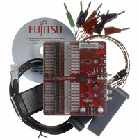
KIT EVAL 16BIT DAC FOR MB86065
Manufacturer
Fujitsu Semiconductor America Inc
Specifications of DK86065-2
Number Of Dac's
1
Number Of Bits
14
Outputs And Type
1, Differential
Sampling Rate (per Second)
1G
Data Interface
Serial
Dac Type
Current
Voltage Supply Source
Analog and Digital
Operating Temperature
-40°C ~ 85°C
Utilized Ic / Part
MB86065
For Use With
865-1111 - DAC DK FPGA ADAPTER BOARD865-1012 - KIT DEV DUAL 14BIT MB86064 SMA
Lead Free Status / RoHS Status
Lead free / RoHS Compliant
Other names
865-1011


September 2007 Version 1.01
FME/MS/DAC80S/DS/5344
MB86065 14-bit 1+GSa/s DAC
6.4
6.4.1 Transformer Coupled Output Circuit
The recommended analog output circuit is a two stage transformer circuit that provides both isolation
from the analog ground plane and excellent common-mode rejection, whilst providing the required
differential to single-ended conversion. The recommended transformers are a Mini-Circuits
(www.minicircuits.com) ADTL1-4-75 transmission line transformer, and an ADT1-1WT balun. See
Figure 22. For best performance the DAC output expects to see a low impedance load.
When considering the recommended circuit, it is important to note that transformer ADT1-1WT is not
exactly 1:1 turns ratio. Instead, when a 50
impedance of approx. 68 is exhibited. Hence, each DAC output sees 33 /34 in parallel with 34 ,
i.e. approx. 16.5 /17 . See Figure 22.
The primary load resistor(s) should be positioned as close as possible to the IOUT and IOUTB balls,
only second in layout priority to the analog decoupling capacitors. The tracking between the DAC and
the resistor(s) should be very closely coupled, ideally as a broadside coupled stacked differential pair
positioned between two ground planes, with low (approx. 33 ) differential impedance tracking.
Where two single-ended load resistors are used these should be closely matched to maximise
CMRR.
The tracking from the termination resistors to the transformer should also be closely coupled, but now
routed adjacent to a ground plane as an edge coupled differential pair for best impedance matching.
Special attention should be paid to the routing of these tracks. The tracks must always be routed as
a matched pair and be equal in length. The routing of these tracks should avoid coming into close
proximity to any power or signal tracks, plane edges or even vias that may cause more noise to be
induced onto one of the tracks than the other. Switching routing layers should be avoided, but if
Copyright © 2004-2007 Fujitsu Microelectronics Europe GmbH
Disclaimer : The contents of this document are subject to change without notice. Customers are advised to consult with FUJITSU sales representatives before
IOUTB
Analog Output Interfacing
ordering.The information and circuit diagrams in this document are presented “as is”, no license is granted by implication or otherwise.
IOUT
The primary load can either be two 33
68
Figure 22 Recommended Transformer Coupled Analog Output Circuit
resistor.
AVSS
33R
33R
or
68R
load is attached to its secondary winding, a primary
33R
33R
10pF
precision resistors to ground or a bridged single
1-4-75
ADTL
Production
AVSS
ADT1-1WT
AVSS
50
Analog Out
Page 45 of 56
Related parts for DK86065-2
Image
Part Number
Description
Manufacturer
Datasheet
Request
R

Part Number:
Description:
IC POWER SUPPLY MONITOR 8SOP
Manufacturer:
Fujitsu Semiconductor America Inc
Datasheet:
Part Number:
Description:
IC POWER SUPPLY MONITOR 8SOP
Manufacturer:
Fujitsu Semiconductor America Inc
Datasheet:

Part Number:
Description:
IC MCU 60K FLASH 2KB RAM 52LQFP
Manufacturer:
Fujitsu Semiconductor America Inc
Datasheet:

Part Number:
Description:
IC MCU 32BIT 256KB FLASH 120LQFP
Manufacturer:
Fujitsu Semiconductor America Inc
Datasheet:
Part Number:
Description:
IC CTLR TOUCH SENSOR 12CH 30SSOP
Manufacturer:
Fujitsu Semiconductor America Inc
Datasheet:

Part Number:
Description:
IC CTLR TOUCH SENSOR 12CH 40QFN
Manufacturer:
Fujitsu Semiconductor America Inc
Datasheet:
Part Number:
Description:
SYNTHESIZER PLL DUAL INP 20SSOP
Manufacturer:
Fujitsu Semiconductor America Inc
Datasheet:

Part Number:
Description:
SYNTHESZR PLL 1.1GHZ DUAL 16SSOP
Manufacturer:
Fujitsu Semiconductor America Inc
Datasheet:

Part Number:
Description:
IC SSCG EMI RED 8-SOIC
Manufacturer:
Fujitsu Semiconductor America Inc
Datasheet:

Part Number:
Description:
IC SSCG EMI RED 8-TSSOP
Manufacturer:
Fujitsu Semiconductor America Inc
Datasheet:

Part Number:
Description:
IC SSCG EMI RED 8-SOP
Manufacturer:
Fujitsu Semiconductor America Inc
Datasheet:

Part Number:
Description:
SYNTHESIZER PLL 2.5GHZ 16SSOP
Manufacturer:
Fujitsu Semiconductor America Inc
Datasheet:
Part Number:
Description:
SYNTHESIZER PLL 1.2GHZ 16SSOP
Manufacturer:
Fujitsu Semiconductor America Inc
Datasheet:

Part Number:
Description:
SYNTHESIZER PLL 2.5GHZ 16BCC
Manufacturer:
Fujitsu Semiconductor America Inc
Datasheet:

Part Number:
Description:
IC SSCG EMI RED 8-SOP
Manufacturer:
Fujitsu Semiconductor America Inc
Datasheet: