DK86064-2 Fujitsu Semiconductor America Inc, DK86064-2 Datasheet - Page 33
DK86064-2
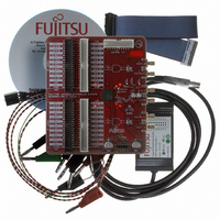
Manufacturer Part Number
DK86064-2
Description
KIT DEB DUAL 14BIT DAC MB86064
Manufacturer
Fujitsu Semiconductor America Inc
Specifications of DK86064-2
Number Of Dac's
2
Number Of Bits
14
Outputs And Type
1, Differential
Sampling Rate (per Second)
1G
Data Interface
Serial
Dac Type
Current
Voltage Supply Source
Analog and Digital
Operating Temperature
-40°C ~ 85°C
Utilized Ic / Part
MB86064
For Use With
865-1111 - DAC DK FPGA ADAPTER BOARD865-1012 - KIT DEV DUAL 14BIT MB86064 SMA
Lead Free Status / RoHS Status
Lead free / RoHS Compliant
Other names
865-1010


October 2005 Version 1.2
FME/MS/DAC80/DS/4972
MB86064 Dual 14-bit 1GSa/s DAC
4.7
4.8
Copyright © 2004-2005 Fujitsu Microelectronics Europe GmbH
Disclaimer : The contents of this document are subject to change without notice. Customers are advised to consult with FUJITSU sales representatives before
Serial Clock Frequency
Setup , SERIAL_IN to SERIAL_CLK rising edge
Hold , SERIAL_IN from SERIAL_CLK rising edge
Delay , SERIAL_CLK to SERIAL_OUT valid
T
1. When programming the WMM on-chip memories F
Power Supply
Power Dissipation
T
1. Current consumption and Power dissipation are data related. Maximum figures are by evaluation.
2. See Figure 17.
3. With WMM enabled power consumption is ~ +76mA / 100MHz (Typ.) +86mA / 100MHz (Max.)
4. See Figure 18.
A
A
Serial Clock Mark or Space
Analog Supply (AVD33)
Digital Supply (DVDD)
Single DAC, 400MHz / 800MSa/s, LVDS data
Dual DAC, 400MHz / 800MSa/s, LVDS data
Single DAC, 500MHz / 1GSa/s, LVDS data
Dual DAC, 400MHz / 800MSa/s, WMM mode
(min) to T
(min) to T
Single DAC, 500MHz / 1GSa/s, LVDS data
Dual DAC, 500MHz / 1GSa/s, LVDS data
Single DAC, 500MHz / 1GSa/s, LVDS data
Dual DAC, 500MHz / 1GSa/s, LVDS data
Serial Interface Timing Specifications
Power Consumption
ordering.The information and circuit diagrams in this document are presented “as is”, no license is granted by implication or otherwise.
A
A
(max), AVD33 = +3.3V, AVSS = 0V, DVDD = +1.8V, DVSS = 0V
(max), AVD33 = +3.3V, AVSS = 0V, DVDD = +1.8V, DVSS = 0V, I
Parameter
Parameter
clk
> 16 x F
Notes
Notes
2, 3
1, 4
1
1
2
2
2
sclk
Symbol
Symbol
V
V
for correct operation.
I
I
AVD33
F
DVDD
t
AVD33
t
DVDD
t
sihld
sisu
P
sov
sclk
D
Production
FS
Min.
Min.
3.1
1.7
20
0
3
3
4
= 20mA.
Ratings
Ratings
1,120
1,660
Typ.
Typ.
140
265
460
650
750
3.3
1.8
83
1,300
1,865
Max.
Max.
106
179
338
587
755
870
3.5
1.9
10
22
Page 33 of 52
Units
Units
MHz
mW
mW
mW
mW
mA
mA
mA
mA
ns
ns
ns
ns
V
V
Related parts for DK86064-2
Image
Part Number
Description
Manufacturer
Datasheet
Request
R

Part Number:
Description:
IC POWER SUPPLY MONITOR 8SOP
Manufacturer:
Fujitsu Semiconductor America Inc
Datasheet:
Part Number:
Description:
IC POWER SUPPLY MONITOR 8SOP
Manufacturer:
Fujitsu Semiconductor America Inc
Datasheet:

Part Number:
Description:
IC MCU 60K FLASH 2KB RAM 52LQFP
Manufacturer:
Fujitsu Semiconductor America Inc
Datasheet:

Part Number:
Description:
IC MCU 32BIT 256KB FLASH 120LQFP
Manufacturer:
Fujitsu Semiconductor America Inc
Datasheet:
Part Number:
Description:
IC CTLR TOUCH SENSOR 12CH 30SSOP
Manufacturer:
Fujitsu Semiconductor America Inc
Datasheet:

Part Number:
Description:
IC CTLR TOUCH SENSOR 12CH 40QFN
Manufacturer:
Fujitsu Semiconductor America Inc
Datasheet:
Part Number:
Description:
SYNTHESIZER PLL DUAL INP 20SSOP
Manufacturer:
Fujitsu Semiconductor America Inc
Datasheet:

Part Number:
Description:
SYNTHESZR PLL 1.1GHZ DUAL 16SSOP
Manufacturer:
Fujitsu Semiconductor America Inc
Datasheet:

Part Number:
Description:
IC SSCG EMI RED 8-SOIC
Manufacturer:
Fujitsu Semiconductor America Inc
Datasheet:

Part Number:
Description:
IC SSCG EMI RED 8-TSSOP
Manufacturer:
Fujitsu Semiconductor America Inc
Datasheet:

Part Number:
Description:
IC SSCG EMI RED 8-SOP
Manufacturer:
Fujitsu Semiconductor America Inc
Datasheet:

Part Number:
Description:
SYNTHESIZER PLL 2.5GHZ 16SSOP
Manufacturer:
Fujitsu Semiconductor America Inc
Datasheet:
Part Number:
Description:
SYNTHESIZER PLL 1.2GHZ 16SSOP
Manufacturer:
Fujitsu Semiconductor America Inc
Datasheet:

Part Number:
Description:
SYNTHESIZER PLL 2.5GHZ 16BCC
Manufacturer:
Fujitsu Semiconductor America Inc
Datasheet:

Part Number:
Description:
IC SSCG EMI RED 8-SOP
Manufacturer:
Fujitsu Semiconductor America Inc
Datasheet: