EVAL-AD5764EBZ Analog Devices Inc, EVAL-AD5764EBZ Datasheet - Page 2
EVAL-AD5764EBZ
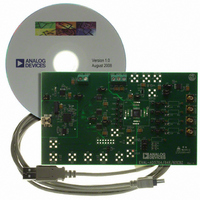
Manufacturer Part Number
EVAL-AD5764EBZ
Description
BOARD EVAL FOR AD5764
Manufacturer
Analog Devices Inc
Specifications of EVAL-AD5764EBZ
Number Of Dac's
4
Number Of Bits
16
Outputs And Type
4, Single Ended
Sampling Rate (per Second)
30M
Data Interface
Serial
Settling Time
8µs
Dac Type
Voltage
Voltage Supply Source
Dual ±
Operating Temperature
-40°C ~ 85°C
Utilized Ic / Part
AD5764
Lead Free Status / RoHS Status
Lead free / RoHS Compliant


AD5764
TABLE OF CONTENTS
Features .............................................................................................. 1
Applications ....................................................................................... 1
General Description ......................................................................... 1
Revision History ............................................................................... 2
Functional Block Diagram .............................................................. 3
Specifications ..................................................................................... 4
Absolute Maximum Ratings ............................................................ 9
Pin Configuration and Function Descriptions ........................... 10
Typical Performance Characteristics ........................................... 12
Terminology .................................................................................... 17
Theory of Operation ...................................................................... 18
REVISION HISTORY
8/09—Rev. C to Rev. D
Changes to Table 2 and Table 3 Endnotes ..................................... 6
Changes to t
1/09—Rev. B to Rev. C
Changes to General Description Section ...................................... 1
Changes to Figure 1 .......................................................................... 3
Changes to Table 2 Conditions ....................................................... 4
Changes to Table 3 Conditions ....................................................... 5
Changes to Table 4 Conditions ....................................................... 6
Changes to Figure 5 .......................................................................... 8
Changes to Table 5 ............................................................................ 9
Changes to Table 6 .......................................................................... 10
Changes to Figure 34 ...................................................................... 19
Changes to Table 7 and Table 10 ................................................... 20
Added Table 8; Renumbered Sequentially .................................. 20
Changes to Table 11 and Table 12 ................................................ 21
Changes to Digital Offset and Gain Control Section ................ 24
Changes to Table 20 ........................................................................ 26
Deleted AD5764 to MC68HC11 Interface Section .................... 27
Deleted Figure 38; Renumbered Sequentially ............................ 27
Deleted AD5764 to 8XC51 Interface Section, Figure 39,
AD5764 to ADSP-2101 Interface Section, Figure 40, and
AD5764 to PIC16C6x/PIC16C7x Interface Section .................. 28
AC Performance Characteristics ................................................ 5
Timing Characteristics ................................................................ 6
ESD Caution .................................................................................. 9
DAC Architecture ....................................................................... 18
Reference Buffers ........................................................................ 18
Serial Interface ............................................................................ 18
Simultaneous Updating via LDAC ........................................... 19
Transfer Function ....................................................................... 20
Asynchronous Clear ( CLR ) ....................................................... 20
6
Parameter and Endnotes, Table 4 ........................... 7
Rev. D | Page 2 of 28
Design Features ............................................................................... 24
Applications Information .............................................................. 25
Layout Guidelines ........................................................................... 27
Outline Dimensions ....................................................................... 28
04/08—Rev. A to Rev. B
Changes to Table Summary Statement, Specifications Section ... 4
Changes to Power Requirements Parameter, Table 2 and
Table Summary Statement ................................................................ 5
Changes to t
Changes to Table 6 .......................................................................... 10
Changed V
Characteristics Section .................................................................. 13
Changes to Table 16 ....................................................................... 22
Changes to Table 18 ....................................................................... 23
Changes to Typical Operating Circuit Section ........................... 28
Changes to AD5764 to ADSP-2101 Section ............................... 29
Changes to Ordering Guide .......................................................... 30
1/07—Rev. 0 to Rev. A
Changes to Absolute Maximum Ratings ..................................... 10
Changes to Figure 25 and Figure 26............................................. 16
3/06—Revision 0: Initial Version
Function Register ....................................................................... 21
Data Register ............................................................................... 21
Coarse Gain Register ................................................................. 21
Fine Gain Register ...................................................................... 22
Offset Register ............................................................................ 22
Offset and Gain Adjustment Worked Example ...................... 23
Analog Output Control ............................................................. 24
Digital Offset and Gain Control ............................................... 24
Programmable Short-Circuit Protection ................................ 24
Digital I/O Port ........................................................................... 24
Local Ground Offset Adjust ...................................................... 24
Typical Operating Circuit ......................................................... 25
Galvanically Isolated Interface ................................................. 27
Microprocessor Interfacing ....................................................... 27
Evaluation Board ........................................................................ 27
Ordering Guide .......................................................................... 28
SS
16
/V
Parameter, Table 4 .................................................... 6
DD
to AV
SS
/AV
DD
in Typical Performance
Related parts for EVAL-AD5764EBZ
Image
Part Number
Description
Manufacturer
Datasheet
Request
R


Part Number:
Description:
BOARD EVAL FOR SI270X-A
Manufacturer:
Silicon Laboratories Inc
Datasheet:

Part Number:
Description:
BUCK CONV REF DESIGN KIT IP1201
Manufacturer:
International Rectifier
Datasheet:
Part Number:
Description:
BOARD DEMO SYNC DUAL BUCK CNVTER
Manufacturer:
International Rectifier
Datasheet:
Part Number:
Description:
BOARD DEMO SYNC BUCK CONVETER
Manufacturer:
International Rectifier
Datasheet:

Part Number:
Description:
EVALBOARD/EB Omnidirectional microphone - Analog
Manufacturer:
Analog Devices
Datasheet:
Part Number:
Description:
EVALBOARD/EB Omnidirectional microphone - Analog
Manufacturer:
Analog Devices
Datasheet:


Part Number:
Description:
BOARD EVAL LED DRIVER LT3756
Manufacturer:
Linear Technology
Datasheet:

Part Number:
Description:
BOARD EVAL FOR AD7741/7742
Manufacturer:
Analog Devices Inc
Datasheet:

Part Number:
Description:
±1.7g Dual-Axis IMEMS Accelerometer Evaluation Board
Manufacturer:
Analog Devices Inc
Datasheet:

Part Number:
Description:
IC MULTIPLIER ANALOG 8-SOIC T/R
Manufacturer:
Analog Devices Inc
Datasheet:

Part Number:
Description:
IC ANALOG MULTIPLIER 8-DIP
Manufacturer:
Analog Devices Inc
Datasheet:
Part Number:
Description:
IC ANALOG MULTIPLIER 8-SOIC
Manufacturer:
Analog Devices Inc
Datasheet:
Part Number:
Description:
IC ANALOG MULTIPLIER 8-DIP
Manufacturer:
Analog Devices Inc
Datasheet: