EVAL-AD5379EBZ Analog Devices Inc, EVAL-AD5379EBZ Datasheet
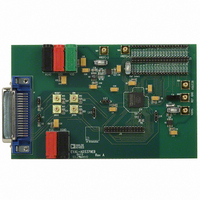
EVAL-AD5379EBZ
Specifications of EVAL-AD5379EBZ


Related parts for EVAL-AD5379EBZ


EVAL-AD5379EBZ Summary of contents
Page 1
FEATURES 40-channel DAC × 108-lead CSPBGA Guaranteed monotonic to 14 bits Buffered voltage outputs Output voltage span of 3.5 V × V (+) REF Maximum output voltage span of 17.5 V System calibration function allowing ...
Page 2
AD5379 TABLE OF CONTENTS Features .............................................................................................. 1 Applications ....................................................................................... 1 General Description ......................................................................... 3 Specifications ..................................................................................... 4 AC Characteristics ........................................................................ 5 Timing Characteristics ..................................................................... 6 Serial Interface .............................................................................. 6 Parallel Interface ........................................................................... 9 Absolute Maximum Ratings .......................................................... 11 ESD Caution ...
Page 3
GENERAL DESCRIPTION The AD5379 contains 40 14-bit DACs in one CSPBGA package. The AD5379 provides a bipolar output range determined by the voltages applied to the V (+) and V (−) inputs. The maxi- REF REF mum output voltage span ...
Page 4
AD5379 SPECIFICATIONS 200 pF to GND kΩ gain = 1; offset ...
Page 5
Parameter 2 Power Supply Sensitivity ∆ Full Scale/∆ ∆ Full Scale/∆ ∆ Full Scale/∆ Power Dissipation Power Dissipation Unloaded (P) Power Dissipation Loaded (P ) TOTAL Junction Temperature ...
Page 6
AD5379 TIMING CHARACTERISTICS SERIAL INTERFACE FIFOEN = 0 V; all specifications T BIAS Table Parameter ...
Page 7
SCLK SYNC DB23 DIN BUSY 1 LDAC VOUT 2 LDAC VOUT t 18 CLR VOUT 1 LDAC ACTIVE DURING BUSY 2 LDAC ACTIVE AFTER BUSY t 25 RESET ...
Page 8
AD5379 SCLK SYNC t 8 DIN D23 INPUT WORD FOR DAC N SDO LDAC BUSY D23' INPUT WORD FOR DAC N D23 UNDEFINED INPUT ...
Page 9
PARALLEL INTERFACE (−) = −3.5 V, FIFOEN = 0 V; all specifications T REF Table Parameter Limit at ...
Page 10
AD5379 REG0, REG1, A7–A02 CS WR DB12–DB0 BUSY 1 LDAC VOUT 2 LDAC VOUT CLR VOUT RESET VOUT BUSY ...
Page 11
ABSOLUTE MAXIMUM RATINGS T = 25°C, unless otherwise noted. A Transient currents 100 mA do not cause SCR latch-up. Table 6. Parameter V to AGND AGND DGND CC Digital Inputs to ...
Page 12
AD5379 PIN CONFIGURATION AND FUNCTION DESCRIPTIONS Table 7. 108-Lead CSPBGA Ball Configuration CSPBGA CSPBGA Number Ball Name Number A1 REG0 DB10 C7 A4 AGND4 BIAS A6 VOUT5 C10 A7 ...
Page 13
Table 8. Pin Function Descriptions Pin Function V (1–3) Logic Power Supply; 2 5.5 V. These pins should be decoupled with 0.1 μF ceramic capacitors and 10 μF CC capacitors. V (1–5) Negative Analog Power Supply; −11.4 V ...
Page 14
AD5379 Pin Function FIFOEN FIFO Enable (Level Sensitive, Active High). When connected to DVDD, the internal FIFO is enabled, allowing the user to write to the device at full speed. FIFO is available in both serial and parallel mode. The ...
Page 15
TERMINOLOGY Relative Accuracy Relative accuracy, or endpoint linearity measure of the maximum deviation from a straight line passing through the endpoints of the DAC transfer function measured after adjusting for zero-scale error and full-scale error and ...
Page 16
AD5379 TYPICAL PERFORMANCE CHARACTERISTICS 1.5 1.0 0.5 0 –0.5 –1.0 –1 AD5379 CODE (10 Figure 8. Typical INL Plot 1400 V = +12V –12V SS 1200 V (+) = +5V ...
Page 17
V = +12V –12V SS 3.0 V (+) = +5V REF V (–) = –3.5V REF 2.5 2.0 1.5 +85°C 1.0 –40°C 0.5 +25°C 0 2.5 3.0 3.5 4.0 4.5 FREQUENCY (MHz) Figure 14. I vs. ...
Page 18
AD5379 FUNCTIONAL DESCRIPTION DAC ARCHITECTURE—GENERAL The AD5379 contains 40 DAC channels and 40 output amplifiers in a single package. The architecture of a single DAC channel consists of a 14-bit resistor-string DAC followed by an output buffer amplifier. The resistor-string ...
Page 19
V FUNCTION BIAS The AD5379 has an on-chip voltage generator that provides a bias voltage of 4.25 V (minimum). The V bypassing and overdriving purposes only not intended to be used as a supply or a reference. If ...
Page 20
AD5379 CALIBRATION The user can perform a system calibration by overwriting the default values in the m and c registers for any individual DAC channel as follows: • Calculate the nominal offset and gain coefficients for the new output range ...
Page 21
FIFO VS. NON-FIFO OPERATION Two modes of operation are available for loading data to the AD5379 registers: operation with FIFO disabled and operation with FIFO enabled. Operation with FIFO disabled is optimum for single writes to the device. If the ...
Page 22
AD5379 INTERFACES The AD5379 contains a serial and a parallel interface. The active interface is selected via the SER/ PAR pin. The AD5379 uses an internal FIFO memory to allow high speed successive writes in both serial and parallel modes. ...
Page 23
Daisy-Chain Mode For systems that contain several DACs, the SDO pin can be used to daisy-chain several devices together. This daisy-chain mode can be useful in system diagnostics and in reducing the number of serial interface lines. Connecting the DCEN ...
Page 24
AD5379 DATA DECODING The AD5379 contains a 14-bit data bus, DB13 to DB0. Depend- ing on the values of REG1 and REG0, this data is loaded into the addressed DAC input register(s), offset (c) register(s), gain (m) register(s), or the ...
Page 25
ADDRESS DECODING The AD5379 contains an 8-bit address bus A0. This address bus allows each DAC input register (x1), each offset (c) register, and each gain (m) register to be individually updated. Table 17. DAC Group Addressing A7 ...
Page 26
AD5379 POWER SUPPLY DECOUPLING In any circuit where accuracy is important, careful considera- tion of the power supply and ground return layout helps to ensure the rated performance. The printed circuit board on which the AD5379 is mounted should be ...
Page 27
TYPICAL APPLICATION CIRCUIT The high channel count of the AD5379 makes it well-suited to applications requiring high levels of integration such as optical and automatic test equipment (ATE) systems. Figure 22 shows the AD5379 as it would be used in ...
Page 28
... ORDERING GUIDE Model Temperature Range AD5379ABC −40°C to +85°C AD5379ABCZ 1 −40°C to +85°C 1 EVAL-AD5379EBZ RoHS Compliant Part. ©2004–2009 Analog Devices, Inc. All rights reserved. Trademarks and registered trademarks are the property of their respective owners. 13.00 BSC BALL A1 INDICATOR 11 ...