EVAL-AD5379EBZ Analog Devices Inc, EVAL-AD5379EBZ Datasheet - Page 19
EVAL-AD5379EBZ
Manufacturer Part Number
EVAL-AD5379EBZ
Description
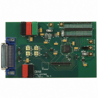
BOARD EVALUATION FOR AD5379
Manufacturer
Analog Devices Inc
Datasheet
1.AD5379ABCZ.pdf
(28 pages)
Specifications of EVAL-AD5379EBZ
Number Of Dac's
40
Number Of Bits
14
Outputs And Type
40, Single Ended
Sampling Rate (per Second)
50k
Data Interface
Serial, Parallel
Settling Time
20µs
Dac Type
Voltage
Voltage Supply Source
Analog and Digital, Dual ±
Operating Temperature
-40°C ~ 85°C
Utilized Ic / Part
AD5379
Lead Free Status / RoHS Status
Lead free / RoHS Compliant


V
The AD5379 has an on-chip voltage generator that provides a
bias voltage of 4.25 V (minimum). The V
bypassing and overdriving purposes only. It is not intended to
be used as a supply or a reference. If V
be pulled high externally to an equal or higher potential (such
as 5 V). The external voltage source should be capable of
driving a 50 μA (typical) current sink load.
REFERENCE SELECTION
The voltages applied to V
output voltage range and span on VOUT0 to VOUT39. If the
offset and gain features are not used (m and c are left at their
power-on values), the required reference levels can be
calculated as follows:
If the offset and gain features of the AD5379 are used, then the
required output range is slightly different. The chosen output
range should take into account the offset and gain errors that
need to be trimmed out. Therefore, the chosen output range
should be larger than the actual, required range.
The required reference levels can be calculated as follows:
1.
2.
3.
4.
5.
In addition, when using reference values other than those
suggested (V
offset error component changes to
where:
V
V
REF
REF
BIAS
(−)
(+)
VREF(+)
VREF(−)
Identify the nominal output range on VOUT.
Identify the maximum offset span and the maximum gain
required on the full output signal range.
Calculate the new maximum output range on VOUT
including the expected, maximum offset and gain errors.
Choose the new required VOUT
the new VOUT limits centered on the nominal values and
assuming REFGND is zero (or equal to AGND). Note that
V
Calculate the values of V
V
V
V
FUNCTION
DD
REF
REF
OFFSET
A
A
(+)
(−)
is the new negative reference value.
is the new positive reference value.
and V
= 0.125 × (V
min
max
REF
min
max
= (VOUT
SS
= (AGND + VOUT
(+) = 5 V and V
= (VOUT
= (AGND + VOUT
must provide sufficient headroom.
max
REF
REF
max
(−)
− VOUT
(+) and V
− VOUT
REF
A
REF
+ 0.7 × V
(+) and V
(−) = −3.5 V), the expected
min
min
min
)/2.5
max
REF
min
REF
)/2.5
)/3.5
(−) determine the
)/3.5
and VOUT
(+) > 4.25 V, V
REF
BIAS
REF
(+)
(−) as follows:
pin is provided for
A
)
min
, keeping
BIAS
must
Rev. B | Page 19 of 28
If this offset error is too large to calibrate, then adjust the
negative reference value to account for this using the following
equation:
Reference Selection Example
Nominal Output Range = 10 V; (−2 V to +8 V)
Offset Error = ±100 mV;
Gain Error = ±3%;
REFGND = AGND = 0 V;
1) Gain Error = ±3%;
=> Maximum Positive Gain Error = +3%
=> Output Range incl. Gain Error = 10 + 0.03(10) = 10.3 V
2) Offset Error = ±100 mV;
=> Maximum Offset Error Span = 2(100) mV = 0.2 V
=> Output Range including Gain Error and
3) V
Actual Output Range = 10.5 V, that is, −2.25 V to +8.25 V
(centered);
=> V
If the solution yields inconvenient reference levels, the user can
adopt one of three approaches:
•
•
•
V
REF
V
Offset Error = 10.3 + 0.2 = 10.5 V
Use a resistor divider to divide down a convenient, higher
reference level to the required level.
Select convenient reference levels above V
V
downsize the references. In this way, the user can use
almost any convenient reference level, but may reduce
performance by overcompaction of the transfer function.
Use a combination of these two approaches.
REF
REF
REF
REF
(+) and V
(−) = −2.25/+2.5 = −0.9 V
(+) = (8.25 + 2.25)/3.5 = 3 V
(−)
(−)
NEW
max
. Modify the gain and offset registers to digitally
= V
REF
(−) Calculation:
REF
(−)
A
− V
OFFSET
/2.625
REF
(+)
AD5379
min
or below
Related parts for EVAL-AD5379EBZ
Image
Part Number
Description
Manufacturer
Datasheet
Request
R


Part Number:
Description:
BOARD EVAL FOR SI270X-A
Manufacturer:
Silicon Laboratories Inc
Datasheet:

Part Number:
Description:
BUCK CONV REF DESIGN KIT IP1201
Manufacturer:
International Rectifier
Datasheet:
Part Number:
Description:
BOARD DEMO SYNC DUAL BUCK CNVTER
Manufacturer:
International Rectifier
Datasheet:
Part Number:
Description:
BOARD DEMO SYNC BUCK CONVETER
Manufacturer:
International Rectifier
Datasheet:

Part Number:
Description:
EVALBOARD/EB Omnidirectional microphone - Analog
Manufacturer:
Analog Devices
Datasheet:
Part Number:
Description:
EVALBOARD/EB Omnidirectional microphone - Analog
Manufacturer:
Analog Devices
Datasheet:


Part Number:
Description:
BOARD EVAL LED DRIVER LT3756
Manufacturer:
Linear Technology
Datasheet:

Part Number:
Description:
BOARD EVAL FOR AD7741/7742
Manufacturer:
Analog Devices Inc
Datasheet:

Part Number:
Description:
±1.7g Dual-Axis IMEMS Accelerometer Evaluation Board
Manufacturer:
Analog Devices Inc
Datasheet:

Part Number:
Description:
IC MULTIPLIER ANALOG 8-SOIC T/R
Manufacturer:
Analog Devices Inc
Datasheet:

Part Number:
Description:
IC ANALOG MULTIPLIER 8-DIP
Manufacturer:
Analog Devices Inc
Datasheet:
Part Number:
Description:
IC ANALOG MULTIPLIER 8-SOIC
Manufacturer:
Analog Devices Inc
Datasheet:
Part Number:
Description:
IC ANALOG MULTIPLIER 8-DIP
Manufacturer:
Analog Devices Inc
Datasheet: