AD8330-EVALZ Analog Devices Inc, AD8330-EVALZ Datasheet - Page 26
AD8330-EVALZ
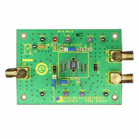
Manufacturer Part Number
AD8330-EVALZ
Description
BOARD EVAL FOR AD8330
Manufacturer
Analog Devices Inc
Specifications of AD8330-EVALZ
Channels Per Ic
1 - Single
Amplifier Type
Variable Gain
Output Type
Differential, Rail-to-Rail
Slew Rate
1500 V/µs
-3db Bandwidth
150MHz
Operating Temperature
-40°C ~ 85°C
Current - Supply (main Ic)
20mA
Voltage - Supply, Single/dual (±)
2.7 V ~ 6 V
Board Type
Fully Populated
Utilized Ic / Part
AD8330
Silicon Manufacturer
Analog Devices
Application Sub Type
Variable Gain Amplifier
Kit Application Type
Amplifier
Silicon Core Number
AD8330
Kit Contents
Board
Lead Free Status / RoHS Status
Lead free / RoHS Compliant
Current - Output / Channel
-
Lead Free Status / RoHS Status
Lead free / RoHS Compliant, Lead free / RoHS Compliant


AD8330
INPUT,
5mV TO 1V rms
When the loop is settled, the average current in Q1 is V
which varies from 2 μA at maximum gain (V
17 μA at minimum gain (V
current causes an increase of ~0.25 dB over the full gain range
in the differential output of nominally 0.75 dBV at midrange
(3.08 V p-p), corresponding to a 200:1 compression ratio. This
is plotted in Figure 65 for a representative 100 kHz input.
The upper panel in Figure 66 shows the time-domain output for
fourteen 3 dB steps in input amplitude from 5.4 mV to 1.7 V.
The waveforms in Figure 65 show the AGC voltage (V
10Ω
0.1µF
1.0
0.9
0.8
0.7
0.6
0.5
–
Figure 65. AGC Output vs. Input Amplitude (Simulation)
5
0
10kΩ
VPSI
INHI
INLO
MODE
R1
ENBL
VDBS
Figure 64. Simple AGC Amplifier (Preliminary)
BIAS AND
VGA CORE
GAIN INTERFACE
–
V-REF
4
0
OFST
CMGN
INPUT TO AD8330 (dBV)
0.1µF
33nF
OFFSET CONTROL
DBS
–30
CM MODE AND
VPOS
= 1.7 V). This change in the Q1
COMM
OUTPUT
STAGES
CONTROL
OUTPUT
–
2
0
CNTR
VMAG
NC
CMOP
VPSO
OPHI
OPLO
DBS
–10
= 0.2 V) to
SEE
TEXT
4.7Ω
0.1µF
Q2
C1
0.1µF
V
DBS
S
Q1
, 2.7V–6V
OUTPUT,
~1V rms
DBS
).
0
/R1,
0.1µF
Rev. E | Page 26 of 32
This simple detector exhibits a temperature variation in the
differential output amplitude of about 4 mV/°C. It provides a
fast attack time (an increase in the input is quickly leveled to the
nominal output, due to the high peak currents in Q1) and a
slow release time (a decrease in the input is not restored as
quickly). The voltage at the VDBS pin can be used as an RSSI
output, scaled 30 mV/dB. Note that the attack time can be
halved by adding a second transistor, labeled Q2 in Figure 64.
For operation at lower frequencies, the AGC hold capacitor
must be increased.
WIDE RANGE TRUE RMS VOLTMETER
The
dynamic range of 60 dB from low frequencies to 2.7 GHz.
This can increase to 110 dB using an AD8330 as a precondi-
tioner, provided the noise bandwidth is limited by an interstage
low-pass or band-pass filter.
The VGA also provides an input port that is easier to drive
than the 200 Ω input of the AD8362. Figure 67 shows the
general scheme.
Both the AD8330 and
interfaces. Thus, when the output of the
the gain of the AD8330, the functional form is unaffected. The
overall scaling is 33 mV/dB. Figure 68 shows the time domain
response using a loop filter capacitor of 10 nF, for inputs rang-
ing from 10 μV to 1 V rms, that is, a 100 dB measurement range.
AD8362
1.75
1.50
1.25
1.00
0.75
0.50
0.25
–1
–2
–3
–4
0
3
2
1
0
0
10
Figure 66. Time Domain Waveforms (Simulation)
is an rms responding detector providing a
V
DBS
20
30
40
AD8362
50
60
TIME
70
provide linear-in-decibel control
80
(µs)
90 100 110 120 130 140 150
AD8362
OUTPUT
is used to control
Related parts for AD8330-EVALZ
Image
Part Number
Description
Manufacturer
Datasheet
Request
R

Part Number:
Description:
BOARD EVAL FOR AD8330
Manufacturer:
Analog Devices Inc
Datasheet:

Part Number:
Description:
±1.7g Dual-Axis IMEMS Accelerometer Evaluation Board
Manufacturer:
Analog Devices Inc
Datasheet:

Part Number:
Description:
Inertial Sensor Evaluation System
Manufacturer:
Analog Devices Inc
Datasheet:
Part Number:
Description:
Manufacturer:
Analog Devices Inc
Datasheet:
Part Number:
Description:
Manufacturer:
Analog Devices Inc
Datasheet:
Part Number:
Description:
Manufacturer:
Analog Devices Inc
Datasheet:
Part Number:
Description:
Manufacturer:
Analog Devices Inc
Datasheet:
Part Number:
Description:
Manufacturer:
Analog Devices Inc
Datasheet:
Part Number:
Description:
Manufacturer:
Analog Devices Inc
Datasheet:
Part Number:
Description:
Manufacturer:
Analog Devices Inc
Datasheet:
Part Number:
Description:
Manufacturer:
Analog Devices Inc
Datasheet:
Part Number:
Description:
Manufacturer:
Analog Devices Inc
Datasheet:
Part Number:
Description:
Manufacturer:
Analog Devices Inc
Datasheet: