AD8260-EVALZ Analog Devices Inc, AD8260-EVALZ Datasheet - Page 22
AD8260-EVALZ
Manufacturer Part Number
AD8260-EVALZ
Description
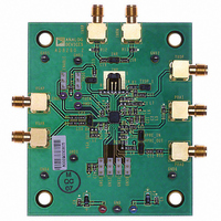
BOARD EVAL FOR AD8260
Manufacturer
Analog Devices Inc
Specifications of AD8260-EVALZ
Channels Per Ic
1 - Single
Amplifier Type
Variable Gain
Output Type
Differential
Slew Rate
730 V/µs
-3db Bandwidth
195MHz
Current - Output / Channel
310mA
Operating Temperature
-40°C ~ 105°C
Current - Supply (main Ic)
28.3mA
Voltage - Supply, Single/dual (±)
3.3 V ~ 10 V, ±3.3 V ~ 5 V
Board Type
Fully Populated
Utilized Ic / Part
AD8260
Silicon Manufacturer
Analog Devices
Application Sub Type
Programmable Gain Amplifier
Kit Application Type
Amplifier
Silicon Core Number
AD8260
Kit Contents
Board
Lead Free Status / RoHS Status
Lead free / RoHS Compliant
Lead Free Status / RoHS Status
Lead free / RoHS Compliant, Lead free / RoHS Compliant


AD8260
PRECAUTIONS TO BE OBSERVED DURING HALF-
DUPLEX OPERATION
During receive, when the high current driver-amplifier is
disabled, its gain setting resistors provide a signal path from
input to output. To prevent inadvertent DAC signals from being
transmitted while receiving via the preamplifier and DGA, the
DAC in Figure 64 must have no output signal.
During transmit, the preamplifier and VGA should be disabled
through any of the nongain-setting codes (see Table 4).
VMID BUFFER
The VMID buffer is a dc bias source that generates the voltage
on Pin 1 and Pin 19, VMDO. Node VMDO cannot accommodate
large dynamic currents and requires excellent ac decoupling to
ground. A high quality 0.1μF capacitor located as close as
possible to Pin 1 and Pin 19 (see Figure 64) is normally sufficient
to decouple the high values of current from Node VMDO.
When operating with dual power supplies, the buffer is disabled
by connecting Pin VMDI, Pin VOCM, and Pin VMDO to ground.
Because the logic decoder in the DGA (GNSx inputs) requires
3.3 V of headroom, the positive supply rails must be 3.3 V or
greater whether single-ended or dual. If a dual supply is used,
the negative rails are the same magnitude (opposite polarity)
as the positive, that is, −3.3 V when VPOS, VPSB, and VPSR
are +3.3 V.
PREAMPLIFIER
The AD8260 includes an uncommitted current feedback op
amp to buffer the resistive attenuator of the DGA. External
resistors are used to adjust the gain. The preamplifier is
characterized with a noninverting gain of 6 dB (2×) and both
gain resistor values of 100 Ω. The preamplifier gain can be
increased using different gain ratios of R
bandwidth and offset voltage. The sum of the values of R
R
be ≥100 Ω because it and an internal compensation capacitor
where:
A
e
e
i
R
A
e
e
e
n,PrA
n
n,PrA
n,RFB1
n,RFB2
n,VGA
FB2
S
t
VGA
,
RS
is the total gain from preamplifier input to the VGA output.
is the source resistance.
should be ≥200 Ω to maintain low distortion. R
is the noise of the source resistance.
is the current noise of the preamplifier at the PRAI pin.
is the input-referred voltage noise of the preamplifier.
e
is the VGA gain.
is the input-referred voltage noise of DGA (low gain output-referred noise divided by a fixed gain of 8×).
is the voltage noise of R
is the voltage noise of R
n
−
out
=
(
e
n
,
RS
×
A
t
)
2
+
(
e
n
FB1
FB2
,
PrA
.
.
×
A
t
)
2
+
FB1
(
i
n
and R
,
PrA
×
FB2
R
S
, trading off
)
FB2
2
+
should
(
e
FB1
n
,
RFB1
and
Rev. A | Page 22 of 32
×
R
R
FB
FB
2
1
×
A
VGA
determine the −3 dB bandwidth of the amplifier. Smaller
resistor values may compromise preamplifier stability.
Because the AD8260 is internally dc-coupled, larger preamplifier
gains increase its offset voltage. The circuit contains an internal
bias resistor and some offset compensation; however, if a lower
value of offset voltage is required, it can be compensated by
connecting a resistor between the FDBK pin and the supply
voltage. If the offset is negative, the resistor value connects to
the negative supply; otherwise, it connects to the positive supply.
For larger gains, the overall noise is reduced if a low value of
R
preamplifier gain is 16× (24.1 dB) and the input-referred noise
is about 1.5 nV/√Hz. For this value of gain, the overall gain range
increases by 18 dB so that the absolute gain range is 12 dB to 42 dB.
PREAMPLIFIER NOISE
The total input-referred voltage and current noise of the positive
input of the preamplifier is about 2.4 nV/√Hz and 5 pA/√Hz,
respectively. The DGA output referred noise is about 25 nV/√Hz
at low gains and 39 nV/√Hz at the highest gain. The 25 nV/√Hz
divided by the DGA fixed gain of 8× results in 3.12 nV/√Hz
referred to the DGA input. Note that this value includes the
noise of the DGA gain setting resistors as well. If this voltage is
divided by the preamplifier gain of 2×, the DGA noise referred
all the way to the preamplifier input is about 1.56 nV/√Hz. From
this, it can be determined that the preamplifier, including the
100 Ω gain setting resistors, contributes about 1.8 nV/√Hz. The
two 100 Ω resistors each contribute 1.29 nV/√Hz at the output
of the preamplifier and 0.9 nV/√Hz referred to the input. With
the gain resistor noise subtracted, the preamplifier noise alone
is about 1.6 nV/√Hz.
Equation 1 shows the calculation that determines the output-
referred noise at maximum gain (24 dB or 16×).
FB1
)
2
is selected. For values of R
+
(
e
n
,
RFB2
×
A
VGA
)
2
+
(
e
n
,
VGA
FB1
×
A
= 20 Ω and R
VGA
)
2
FB2
= 301 Ω, the
(1)
Related parts for AD8260-EVALZ
Image
Part Number
Description
Manufacturer
Datasheet
Request
R

Part Number:
Description:
High Speed, Low Power Dual Operational Amplifier
Manufacturer:
Analog Devices
Datasheet:

Part Number:
Description:
±1.7g Dual-Axis IMEMS Accelerometer Evaluation Board
Manufacturer:
Analog Devices Inc
Datasheet:

Part Number:
Description:
Inertial Sensor Evaluation System
Manufacturer:
Analog Devices Inc
Datasheet:
Part Number:
Description:
Manufacturer:
Analog Devices Inc
Datasheet:
Part Number:
Description:
Manufacturer:
Analog Devices Inc
Datasheet:
Part Number:
Description:
Manufacturer:
Analog Devices Inc
Datasheet:
Part Number:
Description:
Manufacturer:
Analog Devices Inc
Datasheet:
Part Number:
Description:
Manufacturer:
Analog Devices Inc
Datasheet:
Part Number:
Description:
Manufacturer:
Analog Devices Inc
Datasheet:
Part Number:
Description:
Manufacturer:
Analog Devices Inc
Datasheet:
Part Number:
Description:
Manufacturer:
Analog Devices Inc
Datasheet:
Part Number:
Description:
Manufacturer:
Analog Devices Inc
Datasheet:
Part Number:
Description:
Manufacturer:
Analog Devices Inc
Datasheet: