RD3172MMA7455L Freescale Semiconductor, RD3172MMA7455L Datasheet - Page 16
RD3172MMA7455L
Manufacturer Part Number
RD3172MMA7455L
Description
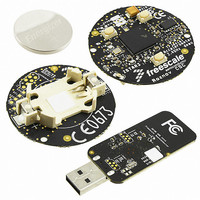
EVAL BOARD FOR MMA7455L
Manufacturer
Freescale Semiconductor
Series
ZSTAR3r
Datasheets
1.RD3172MMA7455L.pdf
(35 pages)
2.RD3172MMA7455L.pdf
(2 pages)
3.RD3172MMA7455L.pdf
(100 pages)
Specifications of RD3172MMA7455L
Design Resources
ZSTAR3 Schematic
Sensor Type
Accelerometer, 3 Axis
Sensing Range
±2g, 4g, 8g
Interface
RF
Sensitivity
16, 32, 64 LSB/g
Voltage - Supply
3V
Embedded
Yes, MCU, 16-Bit
Utilized Ic / Part
MMA7455
Acceleration
5000 g
Sensing Axis
Triple Axis
Output Type
Digital
Interface Type
I2C, SPI
Operating Voltage
3.6 L
Operating Current
490 uA
Maximum Operating Temperature
+ 85 C
Minimum Operating Temperature
- 40 C
Lead Free Status / RoHS Status
Lead free / RoHS Compliant
For Use With/related Products
MMA7455L
Available stocks
Company
Part Number
Manufacturer
Quantity
Price
Company:

Part Number:
RD3172MMA7455L
Manufacturer:
Freescale Semiconductor
Quantity:
135


Detecting Interrupts
LDX
1: Level detection event is detected on X-axis
0: Level detection event is not detected on X-axis
LDY
1: Level detection event is detected on Y-axis
0: Level detection event is not detected on Y-axis
LDZ
1: Level detection event is detected on Z-axis
0: Level detection event is not detected on Z-axis
PDX
1: 1
0: 1
PDY
1: 1
0: 1
DIGITAL INTERFACE
The MMA7455L has both an I
mode of communication. When CS is low, SPI communication is selected. When CS is high, I
Note: It is recommended to disable I
ferent SPI communication protocol. To disable I
I
I
microcontroller, which provides the serial clock signal and addresses the slave device(s) on the bus. The MMA7455L communi-
cates only in slave operation where the device address is $1D. Multiple read and write modes are available. The protocol supports
slave only operation. It does not support Hs mode, “10-bit addressing”, “general call” and: ”START byte”.
SINGLE BYTE READ
The MMA7455L has an 10-bit ADC that can sample, convert and return sensor data on request. The transmission of an 8-bit
command begins on the falling edge of SCL. After the eight clock cycles are used to send the command, note that the data re-
turned is sent with the MSB first once the data is received.
read operation. The Master (or MCU) transmits a start condition (ST) to the MMA7455L, slave address ($1D), with the R/W bit
set to “0” for a write, and the MMA7455L sends an acknowledgement. Then the Master (or MCU) transmits the 8-bit address of
the register to read and the MMA7455L sends an acknowledgement. The Master (or MCU) transmits a repeated start condition
(SR) and then addresses the MMA7455L ($1D) with the R/W bit set to “1” for a read from the previously selected register. The
Slave then acknowledges and transmits the data from the requested register. The Master does not acknowledge (NAK) it re-
ceived the transmitted data, but transmits a stop condition to end the data transfer.
MULTIPLE BYTES READ
The MMA7455L automatically increments the received register address commands after a read command is received. Therefore,
after following the steps of a single byte read, multiple bytes of data can be read from sequential registers after each MMA7455L
acknowledgment (AK) is received until a NACK is received from the Master followed by a stop condition (SP) signalling an end
of transmission. See
$0A: Detection Source Register (Read only)
16
MMA7455L
2
2
C Slave Interface
C is a synchronous serial communication between a master device and one or more slave devices. The master is typically a
st
st
st
st
LDX
D7
pulse is detected on X-axis
pulse is detected on X-axis
pulse is detected on Y-axis
pulse is detected on Y-axis
0
LDY
D6
0
Figure
8.
2
C and SPI digital output available for a communication interface. CS pin is used for selecting the
LDZ
D5
0
2
C during SPI communication to avoid communication errors between devices using a dif-
PDX
2
D4
C, set the I
0
Figure 7
2
CDIS bit in I
PDY
D3
0
PDZ
1: 1
0: 1
INT1
1: Interrupt assigned by INTRG[1:0] bits in Control 1
Register ($18) and is detected
0: Interrupt assigned by INTRG[1:0] bits in Control 1
Register ($18) and is not detected
INT2
1: Interrupt assigned by INTRG[1:0] bits in Control 1
Register ($18) and is detected
0: Interrupt assigned by INTRG[1:0] bits in Control 1
Register ($18) and is not detected
shows the timing diagram for the accelerometer 8-bit I
st
st
pulse is detected on Z-axis
pulse is detected on Z-axis
2
C Device Address register using SPI.
PDZ
D2
0
INT2
D1
0
2
C communication is selected.
Freescale Semiconductor
INT1
D0
0
Reg $0A
Function
Default
Sensors
2
C
Related parts for RD3172MMA7455L
Image
Part Number
Description
Manufacturer
Datasheet
Request
R

Part Number:
Description:
Manufacturer:
Freescale Semiconductor, Inc
Datasheet:
Part Number:
Description:
Manufacturer:
Freescale Semiconductor, Inc
Datasheet:
Part Number:
Description:
Manufacturer:
Freescale Semiconductor, Inc
Datasheet:
Part Number:
Description:
Manufacturer:
Freescale Semiconductor, Inc
Datasheet:
Part Number:
Description:
Manufacturer:
Freescale Semiconductor, Inc
Datasheet:
Part Number:
Description:
Manufacturer:
Freescale Semiconductor, Inc
Datasheet:
Part Number:
Description:
Manufacturer:
Freescale Semiconductor, Inc
Datasheet:
Part Number:
Description:
Manufacturer:
Freescale Semiconductor, Inc
Datasheet:
Part Number:
Description:
Manufacturer:
Freescale Semiconductor, Inc
Datasheet:
Part Number:
Description:
Manufacturer:
Freescale Semiconductor, Inc
Datasheet:
Part Number:
Description:
Manufacturer:
Freescale Semiconductor, Inc
Datasheet:
Part Number:
Description:
Manufacturer:
Freescale Semiconductor, Inc
Datasheet:
Part Number:
Description:
Manufacturer:
Freescale Semiconductor, Inc
Datasheet:
Part Number:
Description:
Manufacturer:
Freescale Semiconductor, Inc
Datasheet:
Part Number:
Description:
Manufacturer:
Freescale Semiconductor, Inc
Datasheet: