RD3172MMA7455L Freescale Semiconductor, RD3172MMA7455L Datasheet - Page 26
RD3172MMA7455L
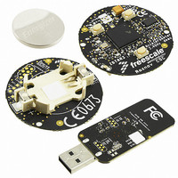
Manufacturer Part Number
RD3172MMA7455L
Description
EVAL BOARD FOR MMA7455L
Manufacturer
Freescale Semiconductor
Series
ZSTAR3r
Datasheets
1.RD3172MMA7455L.pdf
(35 pages)
2.RD3172MMA7455L.pdf
(2 pages)
3.RD3172MMA7455L.pdf
(100 pages)
Specifications of RD3172MMA7455L
Design Resources
ZSTAR3 Schematic
Sensor Type
Accelerometer, 3 Axis
Sensing Range
±2g, 4g, 8g
Interface
RF
Sensitivity
16, 32, 64 LSB/g
Voltage - Supply
3V
Embedded
Yes, MCU, 16-Bit
Utilized Ic / Part
MMA7455
Acceleration
5000 g
Sensing Axis
Triple Axis
Output Type
Digital
Interface Type
I2C, SPI
Operating Voltage
3.6 L
Operating Current
490 uA
Maximum Operating Temperature
+ 85 C
Minimum Operating Temperature
- 40 C
Lead Free Status / RoHS Status
Lead free / RoHS Compliant
For Use With/related Products
MMA7455L
Available stocks
Company
Part Number
Manufacturer
Quantity
Price
Company:

Part Number:
RD3172MMA7455L
Manufacturer:
Freescale Semiconductor
Quantity:
135


Table 12. Configuring the Interrupt settings using Register $18 with INTREG[1:0] bits
$17: Interrupt Latch Reset (Read/Write)
CLR_INT1
CLR_INT2
00: INT1 Register is detecting Level while INT2 is detecting Pulse.
01: INT1 Register is detecting Pulse while INT2 is detecting Level.
10: INT1 Register is detecting a Single Pulse and INT2 is detecting Single Pulse (if 2
time window and second time window > 0 then INT2 will detect the double pulse only.
INTPIN: INT1 pin is routed to INT1 bit in Detection Source Register ($0A) and INT2 pin is routed to INT2 bit in Detection Source
Register ($0A).
INTPIN: INT2 pin is routed to INT1 bit in Detection Source Register ($0A) and INT1 pin is routed to INT2 bit in Detection Source
Register ($0A).
XDA
1: X-axis is disabled for detection.
0: X-axis is enabled for detection.
YDA
1: Y-axis is disabled for detection.
0: Y-axis is enabled for detection.
ZDA
1: Z-axis is disabled for detection.
0: Z-axis is enabled for detection.
$19: Control 2 (Read/Write)
LDPL
0: Level detection polarity is positive and detecting condition
is OR 3 axes.
1: Level detection polarity is negative detecting condition is
AND 3 axes.
$18 Control 1 (Read/Write)
26
MMA7455L
DFBW
D7
D7
D7
--
0
0
0
INTREG[1:0]
1: Clear “INT1” and LDX/LDY/LDZ or PDX/PDY/PDZ bits in Detection Source Register ($0A) depending on
Control1($18) INTREG[1:0] setting.
0: Do not clear “INT1” LDX/LDY/LDZ or PDX/PDY/PDZ bits in Detection Source Register ($0A)
1: Clear “INT2” and LDX/LDY/LDZ or PDX/PDY/PDZ bits in Detection Source Register ($0A) depending on
Control1($18) INTREG[1:0] setting.
0: Do not clear “INT2” and LDX/LDY/LDZ or PDX/PDY/PDZ bits in Detection Source Register ($0A).
00
01
10
THOPT
D6
D6
D6
--
0
0
0
ZDA
D5
D5
D5
--
0
0
0
Single Pulse detection
“INT1” Register Bit
Pulse Detection
Level detection
YDA
D4
D4
D4
--
0
0
0
XDA
D3
D3
D3
0
--
0
0
THOPT (This bit is valid for level detection only, not valid
DFBW
0: Digital filter band width is 62.5 Hz
1: Digital filter band width is 125 Hz
PDPL
0: Pulse detection polarity is positive and detecting condition
is OR 3 axes.
1: Pulse detection polarity is negative and detecting condition
is AND 3 axes.
DRVO
0: Standard drive strength on SDA/SDO pin
1: Strong drive strength on SDA/SDO pin
0: Threshold value is absolute only
1: Integer value is available.
for pulse detection)
INTREG[1]
DRVO
D2
D2
D2
0
--
0
0
nd
Time Window = 0) or if there is a latency
INTREG[0]
CLR_INT2
Single or Double Pulse Detection
PDPL
D1
D1
D1
0
0
0
“INT2” Register Bit
Pulse Detection
Level Detection
CLR_INT1
Freescale Semiconductor
INTPIN
LDPL
D0
D0
D0
0
0
0
Function
Function
Function
Default
Default
Default
Bit
Bit
Bit
Sensors
Related parts for RD3172MMA7455L
Image
Part Number
Description
Manufacturer
Datasheet
Request
R

Part Number:
Description:
Manufacturer:
Freescale Semiconductor, Inc
Datasheet:
Part Number:
Description:
Manufacturer:
Freescale Semiconductor, Inc
Datasheet:
Part Number:
Description:
Manufacturer:
Freescale Semiconductor, Inc
Datasheet:
Part Number:
Description:
Manufacturer:
Freescale Semiconductor, Inc
Datasheet:
Part Number:
Description:
Manufacturer:
Freescale Semiconductor, Inc
Datasheet:
Part Number:
Description:
Manufacturer:
Freescale Semiconductor, Inc
Datasheet:
Part Number:
Description:
Manufacturer:
Freescale Semiconductor, Inc
Datasheet:
Part Number:
Description:
Manufacturer:
Freescale Semiconductor, Inc
Datasheet:
Part Number:
Description:
Manufacturer:
Freescale Semiconductor, Inc
Datasheet:
Part Number:
Description:
Manufacturer:
Freescale Semiconductor, Inc
Datasheet:
Part Number:
Description:
Manufacturer:
Freescale Semiconductor, Inc
Datasheet:
Part Number:
Description:
Manufacturer:
Freescale Semiconductor, Inc
Datasheet:
Part Number:
Description:
Manufacturer:
Freescale Semiconductor, Inc
Datasheet:
Part Number:
Description:
Manufacturer:
Freescale Semiconductor, Inc
Datasheet:
Part Number:
Description:
Manufacturer:
Freescale Semiconductor, Inc
Datasheet: