TOOLSTICK540DC Silicon Laboratories Inc, TOOLSTICK540DC Datasheet - Page 61
TOOLSTICK540DC
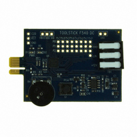
Manufacturer Part Number
TOOLSTICK540DC
Description
DAUGHTER CARD TOOLSTICK F540
Manufacturer
Silicon Laboratories Inc
Series
ToolStickr
Type
MCUr
Datasheets
1.TOOLSTICK540DC.pdf
(274 pages)
2.TOOLSTICK540DC.pdf
(16 pages)
3.TOOLSTICK540DC.pdf
(12 pages)
Specifications of TOOLSTICK540DC
Contents
Daughter Card
Processor To Be Evaluated
C8051F54x
Processor Series
C8051F54x
Interface Type
USB
Operating Supply Voltage
2.7 V to 3.6 V
Lead Free Status / RoHS Status
Lead free / RoHS Compliant
For Use With/related Products
C8051F54x
For Use With
336-1345 - TOOLSTICK BASE ADAPTER336-1182 - ADAPTER USB DEBUG FOR C8051FXXX
Lead Free Status / Rohs Status
Lead free / RoHS Compliant
Other names
336-1717


7. Voltage Reference
The Voltage reference multiplexer on the C8051F54x devices is configurable to use an externally con-
nected voltage reference, the on-chip reference voltage generator routed to the VREF pin, or the V
power supply voltage (see Figure 7.1). The REFSL bit in the Reference Control register (REF0CN, SFR
Definition 7.1) selects the reference source for the ADC. For an external source or the on-chip reference,
REFSL should be set to 0 to select the VREF pin. To use V
set to 1.
The BIASE bit enables the internal voltage bias generator, which is used by the ADC, Temperature Sensor,
and internal oscillator. This bias is automatically enabled when any peripheral which requires it is enabled,
and it does not need to be enabled manually. The bias generator may be enabled manually by writing a 1
to the BIASE bit in register REF0CN. The electrical specifications for the voltage reference circuit are given
in Table 6.11.
The on-chip voltage reference circuit consists of a temperature stable bandgap voltage reference genera-
tor and a gain-of-two output buffer amplifier. The output voltage is selectable between 1.5 V and 2.25 V.
The on-chip voltage reference can be driven on the VREF pin by setting the REFBE bit in register REF0CN
to a 1. The maximum load seen by the VREF pin must be less than 200 µA to GND. Bypass capacitors of
0.1 µF and 4.7 µF are recommended from the VREF pin to GND. If the on-chip reference is not used, the
REFBE bit should be cleared to 0. Electrical specifications for the on-chip voltage reference are given in
Table 6.11.
Important Note about the VREF Pin: When using either an external voltage reference or the on-chip ref-
erence circuitry, the VREF pin should be configured as an analog pin and skipped by the Digital Crossbar.
Refer to Section “18. Port Input/Output” on page 147 for the location of the VREF pin, as well as details of
how to configure the pin in analog mode and to be skipped by the crossbar.
GND
VDD
4.7F
Recommended Bypass
R1
Figure 7.1. Voltage Reference Functional Block Diagram
Capacitors
+
Reference
External
Voltage
Circuit
0.1F
VREF
VDD
REF0CN
Rev. 1.1
0
1
IOSCE
N
Reference
DD
REFBE
Internal
EN
as the reference source, REFSL should be
EN
EN
Bias Generator
Temp Sensor
To Analog Mux
(to ADC)
C8051F54x
VREF
To ADC, Internal
Oscillators
DD
61
Related parts for TOOLSTICK540DC
Image
Part Number
Description
Manufacturer
Datasheet
Request
R

Part Number:
Description:
KIT TOOL EVAL SYS IN A USB STICK
Manufacturer:
Silicon Laboratories Inc
Datasheet:

Part Number:
Description:
TOOLSTICK DEBUG ADAPTER
Manufacturer:
Silicon Laboratories Inc
Datasheet:

Part Number:
Description:
TOOLSTICK BASE ADAPTER
Manufacturer:
Silicon Laboratories Inc
Datasheet:

Part Number:
Description:
TOOLSTICK DAUGHTER CARD
Manufacturer:
Silicon Laboratories Inc
Datasheet:

Part Number:
Description:
TOOLSTICK DAUGHTER CARD
Manufacturer:
Silicon Laboratories Inc
Datasheet:

Part Number:
Description:
TOOLSTICK DAUGHTER CARD
Manufacturer:
Silicon Laboratories Inc
Datasheet:

Part Number:
Description:
TOOLSTICK PROGRAMMING ADAPTER
Manufacturer:
Silicon Laboratories Inc
Datasheet:

Part Number:
Description:
TOOLSTICK DAUGHTER CARD
Manufacturer:
Silicon Laboratories Inc
Datasheet:

Part Number:
Description:
KIT STARTER TOOLSTICK
Manufacturer:
Silicon Laboratories Inc
Datasheet:

Part Number:
Description:
KIT UNIVERSITY TOOLSTICK STARTER
Manufacturer:
Silicon Laboratories Inc
Datasheet:

Part Number:
Description:
DAUGHTER CARD TOOLSTICK F330
Manufacturer:
Silicon Laboratories Inc
Datasheet:

Part Number:
Description:
CARD DAUGHTER UNIVRSTY TOOLSTICK
Manufacturer:
Silicon Laboratories Inc
Datasheet:

Part Number:
Description:
DAUGHTER CARD TOOLSTICK F582
Manufacturer:
Silicon Laboratories Inc
Datasheet:

Part Number:
Description:
DAUGHTER CARD TOOLSTICK F500
Manufacturer:
Silicon Laboratories Inc
Datasheet:

Part Number:
Description:
DAUGHTER CARD TOOLSTICK F560
Manufacturer:
Silicon Laboratories Inc
Datasheet: