TOOLSTICK540DC Silicon Laboratories Inc, TOOLSTICK540DC Datasheet - Page 72
TOOLSTICK540DC
Manufacturer Part Number
TOOLSTICK540DC
Description
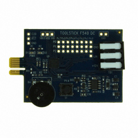
DAUGHTER CARD TOOLSTICK F540
Manufacturer
Silicon Laboratories Inc
Series
ToolStickr
Type
MCUr
Datasheets
1.TOOLSTICK540DC.pdf
(274 pages)
2.TOOLSTICK540DC.pdf
(16 pages)
3.TOOLSTICK540DC.pdf
(12 pages)
Specifications of TOOLSTICK540DC
Contents
Daughter Card
Processor To Be Evaluated
C8051F54x
Processor Series
C8051F54x
Interface Type
USB
Operating Supply Voltage
2.7 V to 3.6 V
Lead Free Status / RoHS Status
Lead free / RoHS Compliant
For Use With/related Products
C8051F54x
For Use With
336-1345 - TOOLSTICK BASE ADAPTER336-1182 - ADAPTER USB DEBUG FOR C8051FXXX
Lead Free Status / Rohs Status
Lead free / RoHS Compliant
Other names
336-1717


C8051F54x
9. Voltage Regulator (REG0)
C8051F54x devices include an on-chip low dropout voltage regulator (REG0). The input to REG0 at the
V
enabled, the output of REG0 appears on the V
power external devices. On reset, REG0 is enabled and can be disabled by software.
The Voltage regulator can generate an interrupt (if enabled by EREG0, EIE2.0) that is triggered whenever
the V
flag and the recommended procedure to use it is as follows:
1. Wait enough time to ensure the V
2. Enable the dropout interrupt (EREG0, EIE2.0) and select the proper priority (PREG0, EIP2.0)
3. If triggered, inside the interrupt disable it (clear EREG0, EIE2.0), execute all procedures necessary to
4. In the main application, now running in the safe mode, regularly check the DROPOUT bit (REG0CN.0).
The input (V
tor (4.7 µF + 0.1 µF) to ground as shown in Figure 9.1 below. This capacitor will eliminate power spikes
and provide any immediate power required by the microcontroller. The settling time associated with the
voltage regulator is shown in Table 6.8 on page 54.
If the internal voltage regulator is not used, the V
72
REGIN
protect your application (put it in a safe mode and leave the interrupt now disabled).
Once it is cleared by the regulator hardware, the application can enable the interrupt again (EREG0,
EIE1.6) and return to the normal mode operation.
REGIN
pin can be as high as 5.25 V. The output can be selected by software to 2.1 V or 2.6 V. When
input voltage drops below the dropout threshold voltage. This dropout interrupt has no pending
REGIN
Figure 9.1. External Capacitors for Voltage Regulator Input/Output—
) and output (V
REG0
V
DD
DD
) of the voltage regulator should both be bypassed with a large capaci-
4.7 µF
4.7 µF
REGIN
Regulator Enabled
input voltage is stable
DD
REGIN
Rev. 1.1
pin, powers the microcontroller core, and can be used to
input should be tied to V
.1 µF
.1 µF
V
V
DD
REGIN
DD
, as shown in Figure 9.2.
Related parts for TOOLSTICK540DC
Image
Part Number
Description
Manufacturer
Datasheet
Request
R

Part Number:
Description:
KIT TOOL EVAL SYS IN A USB STICK
Manufacturer:
Silicon Laboratories Inc
Datasheet:

Part Number:
Description:
TOOLSTICK DEBUG ADAPTER
Manufacturer:
Silicon Laboratories Inc
Datasheet:

Part Number:
Description:
TOOLSTICK BASE ADAPTER
Manufacturer:
Silicon Laboratories Inc
Datasheet:

Part Number:
Description:
TOOLSTICK DAUGHTER CARD
Manufacturer:
Silicon Laboratories Inc
Datasheet:

Part Number:
Description:
TOOLSTICK DAUGHTER CARD
Manufacturer:
Silicon Laboratories Inc
Datasheet:

Part Number:
Description:
TOOLSTICK DAUGHTER CARD
Manufacturer:
Silicon Laboratories Inc
Datasheet:

Part Number:
Description:
TOOLSTICK PROGRAMMING ADAPTER
Manufacturer:
Silicon Laboratories Inc
Datasheet:

Part Number:
Description:
TOOLSTICK DAUGHTER CARD
Manufacturer:
Silicon Laboratories Inc
Datasheet:

Part Number:
Description:
KIT STARTER TOOLSTICK
Manufacturer:
Silicon Laboratories Inc
Datasheet:

Part Number:
Description:
KIT UNIVERSITY TOOLSTICK STARTER
Manufacturer:
Silicon Laboratories Inc
Datasheet:

Part Number:
Description:
DAUGHTER CARD TOOLSTICK F330
Manufacturer:
Silicon Laboratories Inc
Datasheet:

Part Number:
Description:
CARD DAUGHTER UNIVRSTY TOOLSTICK
Manufacturer:
Silicon Laboratories Inc
Datasheet:

Part Number:
Description:
DAUGHTER CARD TOOLSTICK F582
Manufacturer:
Silicon Laboratories Inc
Datasheet:

Part Number:
Description:
DAUGHTER CARD TOOLSTICK F500
Manufacturer:
Silicon Laboratories Inc
Datasheet:

Part Number:
Description:
DAUGHTER CARD TOOLSTICK F560
Manufacturer:
Silicon Laboratories Inc
Datasheet: