AD9777-EB Analog Devices Inc, AD9777-EB Datasheet - Page 20
AD9777-EB
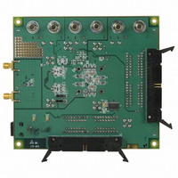
Manufacturer Part Number
AD9777-EB
Description
BOARD EVAL FOR AD9777
Manufacturer
Analog Devices Inc
Series
TxDAC+®r
Datasheet
1.AD9777BSVZ.pdf
(60 pages)
Specifications of AD9777-EB
Rohs Status
RoHS non-compliant
Number Of Dac's
2
Number Of Bits
16
Outputs And Type
2, Differential
Sampling Rate (per Second)
160M
Data Interface
Parallel
Settling Time
11ns
Dac Type
Current
Voltage Supply Source
Analog and Digital
Operating Temperature
-40°C ~ 85°C
Utilized Ic / Part
AD9777


AD9777
REGISTER DESCRIPTION
Address 00h
Bit 7: Logic 0 (default) causes the SPI_SDIO pin to act as an
input during the data transfer (Phase 2) of the communications
cycle. When set to 1, SPI_SDIO can act as an input or output,
depending on Bit 7 of the instruction byte.
Bit 6: Logic 0 (default). Determines the direction (LSB/MSB
first) of the communications and data transfer communications
cycles. Refer to the MSB/LSB Transfers section for more details.
Bit 5: Writing a 1 to this bit resets the registers to their default
values and restarts the chip. The RESET bit always reads back 0.
Register Address 00h bits are not cleared by this software reset.
However, a high level at the RESET pin forces all registers,
including those in Address 00h, to their default state.
Bit 4: Sleep Mode. A Logic 1 to this bit shuts down the DAC
output currents.
Bit 3: Power-Down. Logic 1 shuts down all analog and digital
functions except for the SPI port.
Bit 2: 1R/2R Mode. The default (0) places the AD9777 in two
resistor mode. In this mode, the I
DAC references are set separately by the R
FSADJ2 and FSADJ1 (Pins 59 and 60). In 2R mode, assuming
the coarse gain setting is full scale and the fine gain setting is 0,
I
V
both I and Q DACs are controlled by a single resistor on Pin 60.
I
of what it would be in 2R mode, assuming all other conditions
(R
current of each DAC can still be set to 20 mA by choosing a
resistor of half the value of the R
Bit 1: PLL_LOCK Indicator. When the PLL is enabled, reading
this bit gives the status of the PLL. A Logic 1 indicates the PLL
is locked. A Logic 0 indicates an unlocked state.
Address 01h
Bit 7, Bit 6: This is the filter interpolation rate according to the
following table.
00
01
10
11
Bit 5 and Bit 4: This is the modulation mode according to the
following table.
00
01
10
11
FULLSCALE1
FULLSCALE
REF
SET
/FSADJ2. With this bit set to 1, the reference currents for
, register settings) remain unchanged. The full-scale
in one resistor mode for both the I and Q DACs is half
= 32 × V
REF
1×
2×
4×
8×
none
f
f
f
S
S
S
/2
/4
/8
/FSADJ1 and I
SET
REF
value used in 2R mode.
FULLSCALE2
currents for the I and Q
SET
= 32 ×
resistors on
Rev. C | Page 20 of 60
Bit 3: Logic 1 enables zero stuffing mode for interpolation filters.
Bit 2: Default (1) enables the real mix mode. The I and Q data
channels are individually modulated by f
the interpolation filters. However, no complex modulation is
done. In the complex mix mode (Logic 0), the digital
modulators on the I and Q data channels are coupled to create a
digital complex modulator. When the AD9777 is applied in
conjunction with an external quadrature modulator, rejection
can be achieved of either the higher or lower frequency image
around the second IF frequency (that is, the LO of the analog
quadrature modulator external to the AD9777) according to the
bit value of Register 01h, Bit 1.
Bit 1: Logic 0 (default) causes the complex modulation to be of
the form e
image when the AD9777 is used with an external quadrature
modulator. A Logic 1 causes the modulation to be of the form
e
Bit 0: In two-port mode, a Logic 0 (default) causes Pin 8 to act
as a lock indicator for the internal PLL. A Logic 1 in this register
causes Pin 8 to act as a DATACLK. For more information, see
the Two Port Data Input Mode section.
Address 02h
Bit 7: Logic 0 (default) causes data to be accepted on the inputs
as twos complement binary. Logic 1 causes data to be accepted
as straight binary.
Bit 6: Logic 0 (default) places the AD9777 in two-port mode. I
and Q data enters the AD9777 via Ports 1 and 2, respectively. A
Logic 1 places the AD9777 in one-port mode in which
interleaved I and Q data is applied to Port 1. See Table 8 for
detailed information on how to use the DATACLK/PLL_LOCK,
IQSEL, and ONEPORTCLK modes.
Bit 5: DATACLK Driver Strength. With the internal PLL
disabled and this bit set to Logic 0, it is recommended that
DATACLK be buffered. When this bit is set to Logic 1,
DATACLK acts as a stronger driver capable of driving small
capacitive loads.
Bit 4: Logic 0 (default). A value of 1 inverts DATACLK at Pin 8.
Bit 2: Logic 0 (default). A value of 1 inverts ONEPORTCLK
at Pin 32.
Bit 1: Logic 0 (default) causes IQSEL = 0 to direct input data to
the I channel, while IQSEL = 1 directs input data to the Q
channel.
Bit 0: Logic 0 (default) defines IQ pairing as IQ, IQ…, while
programming a Logic 1 causes the pair ordering to
be QI, QI…
+jωt
, which causes rejection of the lower frequency image.
−jωt
, resulting in the rejection of the higher frequency
S
/2, f
S
/4, or f
S
/8 after
Related parts for AD9777-EB
Image
Part Number
Description
Manufacturer
Datasheet
Request
R

Part Number:
Description:
16Bit 400 MSPS Dual TxDAC+ D/A Converter
Manufacturer:
Analog Devices Inc
Datasheet:

Part Number:
Description:
±1.7g Dual-Axis IMEMS Accelerometer Evaluation Board
Manufacturer:
Analog Devices Inc
Datasheet:
Part Number:
Description:
Inertial Sensor Evaluation System
Manufacturer:
Analog Devices Inc
Datasheet:
Part Number:
Description:
Manufacturer:
Analog Devices Inc
Datasheet:
Part Number:
Description:
Manufacturer:
Analog Devices Inc
Datasheet:
Part Number:
Description:
Manufacturer:
Analog Devices Inc
Datasheet:
Part Number:
Description:
Manufacturer:
Analog Devices Inc
Datasheet:
Part Number:
Description:
Manufacturer:
Analog Devices Inc
Datasheet:
Part Number:
Description:
Manufacturer:
Analog Devices Inc
Datasheet:
Part Number:
Description:
Manufacturer:
Analog Devices Inc
Datasheet:
Part Number:
Description:
Manufacturer:
Analog Devices Inc
Datasheet:
Part Number:
Description:
Manufacturer:
Analog Devices Inc
Datasheet:
Part Number:
Description:
Manufacturer:
Analog Devices Inc
Datasheet: