EVAL-AD7655CB Analog Devices Inc, EVAL-AD7655CB Datasheet - Page 25
EVAL-AD7655CB
Manufacturer Part Number
EVAL-AD7655CB
Description
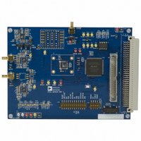
BOARD EVAL FOR AD7655
Manufacturer
Analog Devices Inc
Series
PulSAR®r
Specifications of EVAL-AD7655CB
Number Of Adc's
1
Number Of Bits
16
Sampling Rate (per Second)
1M
Data Interface
Serial, Parallel
Inputs Per Adc
4 Single Ended
Input Range
0 ~ 2 V
Power (typ) @ Conditions
120mW @ 1MSPS
Voltage Supply Source
Analog and Digital
Operating Temperature
-40°C ~ 85°C
Utilized Ic / Part
AD7655
Lead Free Status / RoHS Status
Contains lead / RoHS non-compliant


APPLICATION HINTS
LAYOUT
The AD7655 has very good immunity to noise on the power
supplies. However, care should still be taken with regard to
grounding layout.
The printed circuit board that houses the AD7655 should be
designed so the analog and digital sections are separated and
confined to certain areas of the board. This facilitates the use of
ground planes that can be separated easily. Digital and analog
ground planes should be joined in only one place, preferably
underneath the AD7655, or as close as possible to the AD7655.
If the AD7655 is in a system where multiple devices require
analog-to-digital ground connections, the connection should
still be made at one point only, a star ground point that should
be established as close as possible to the AD7655.
Avoid unning digital lines under the device because these
couple noise onto the die. The analog ground plane should be
allowed to run under the AD7655 to avoid noise coupling. Fast
switching signals such as CNVST or clocks should be shielded
with digital ground to avoid radiating noise to other sections of
the board and should never run near analog signal paths.
Crossover of digital and analog signals should be avoided.
Traces on different but close layers of the board should run at
right angles to each other. This reduces the effect of crosstalk
through the board.
The power supply lines to the AD7655 should use as large a
trace as possible to provide low impedance paths and reduce the
effect of glitches on the power supply lines. Good decoupling is
also important to lower the supply impedance presented to the
AD7655 and to reduce the magnitude of the supply spikes.
Decoupling ceramic capacitors, typically 100 nF, should be
Rev. B | Page 25 of 28
placed on each power supply pin—AVDD, DVDD, and
OVDD—close to, and ideally right up against these pins and
their corresponding ground pins. Additionally, low ESR 10 μF
capacitors should be located near the ADC to further reduce
low frequency ripple.
The DVDD supply of the AD7655 can be a separate supply or
can come from the analog supply AVDD or the digital interface
supply OVDD. When the system digital supply is noisy or when
fast switching digital signals are present, if no separate supply is
available, the user should connect DVDD to AVDD through an
RC filter (see Figure 17) and the system supply to OVDD and
the remaining digital circuitry. When DVDD is powered from
the system supply, it is useful to insert a bead to further reduce
high frequency spikes.
The AD7655 has five ground pins: INGND, REFGND, AGND,
DGND, and OGND. INGND is used to sense the analog input
signal. REFGND senses the reference voltage and, because it
carries pulsed currents, should be a low impedance return to
the reference. AGND is the ground to which most internal
ADC analog signals are referenced; it must be connected with
the least resistance to the analog ground plane. DGND must be
tied to the analog or digital ground plane depending on the
configuration. OGND is connected to the digital system
ground.
EVALUATING THE AD7655 PERFORMANCE
A recommended layout for the AD7655 is outlined in the
EVAL-AD7655CB evaluation board documentation. The
evaluation board package includes a fully assembled and tested
evaluation board, documentation, and software for controlling
the board from a PC via the EVAL-CONTROL-BRD3.
AD7655
Related parts for EVAL-AD7655CB
Image
Part Number
Description
Manufacturer
Datasheet
Request
R

Part Number:
Description:
ENERCHIP CC EVAL KIT
Manufacturer:
Cymbet Corporation
Datasheet:

Part Number:
Description:
BOARD EVAL FOR AD976
Manufacturer:
Analog Devices Inc
Datasheet:

Part Number:
Description:
BOARD EVAL FOR ADXL345
Manufacturer:
Analog Devices Inc
Datasheet:

Part Number:
Description:
ENERCHIP CC SEH EVAL KIT
Manufacturer:
Cymbet Corporation
Datasheet:

Part Number:
Description:
ENERCHIP EP ENERGY HARVEST EVAL
Manufacturer:
Cymbet Corporation
Datasheet:

Part Number:
Description:
EVAL BOARD FOR TW6864-LB2-GR
Manufacturer:
Intersil
Datasheet:
Part Number:
Description:
EVAL BOARD FOR TW8816-LB3-GR
Manufacturer:
Intersil
Datasheet:
Part Number:
Description:
EVAL BOARD FOR TW8817-TA3-GRS
Manufacturer:
Intersil
Datasheet:

Part Number:
Description:
EVALUATION MODULE FOR ADUM4160
Manufacturer:
Analog Devices Inc
Datasheet:

Part Number:
Description:
BOARD EVALUATION ADCMP581BCP
Manufacturer:
Analog Devices Inc
Datasheet:
Part Number:
Description:
BOARD EVALUATION ADM1041
Manufacturer:
Analog Devices Inc
Datasheet:

Part Number:
Description:
EVAL BOARD FOR STM32F107VCT
Manufacturer:
STMicroelectronics
Datasheet:
Part Number:
Description:
BOARD EVAL FOR AD1954
Manufacturer:
Analog Devices Inc
Datasheet:
Part Number:
Description:
BOARD EVAL FOR AD1955
Manufacturer:
Analog Devices Inc
Datasheet:

Part Number:
Description:
BOARD EVAL FOR AD9831
Manufacturer:
Analog Devices Inc
Datasheet: