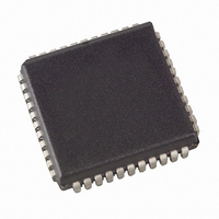
AT89LS52-16JU Atmel, AT89LS52-16JU Datasheet - Page 21

AT89LS52-16JU
Manufacturer Part Number
AT89LS52-16JU
Description
IC MCU 8K FLASH 16MHZ 44-PLCC
Manufacturer
Atmel
Series
89LSr
Datasheet
1.AT89LS52-16JU.pdf
(39 pages)
Specifications of AT89LS52-16JU
Core Processor
8051
Core Size
8-Bit
Speed
16MHz
Connectivity
UART/USART
Peripherals
WDT
Number Of I /o
32
Program Memory Size
8KB (8K x 8)
Program Memory Type
FLASH
Ram Size
256 x 8
Voltage - Supply (vcc/vdd)
2.7 V ~ 4 V
Oscillator Type
Internal
Operating Temperature
-40°C ~ 85°C
Package / Case
44-PLCC
Processor Series
AT89x
Core
8051
Data Bus Width
8 bit
Data Ram Size
256 B
Interface Type
UART
Maximum Clock Frequency
16 MHz
Number Of Programmable I/os
32
Number Of Timers
3
Operating Supply Voltage
2.7 V to 4 V
Maximum Operating Temperature
+ 85 C
Mounting Style
SMD/SMT
3rd Party Development Tools
PK51, CA51, A51, ULINK2
Development Tools By Supplier
AT89ISP
Minimum Operating Temperature
- 40 C
Cpu Family
89LS
Device Core
8051
Device Core Size
8b
Frequency (max)
16MHz
Total Internal Ram Size
256Byte
# I/os (max)
32
Number Of Timers - General Purpose
3
Operating Supply Voltage (typ)
3.3V
Operating Supply Voltage (max)
4V
Operating Supply Voltage (min)
2.7V
Instruction Set Architecture
CISC
Operating Temp Range
-40C to 85C
Operating Temperature Classification
Industrial
Mounting
Surface Mount
Pin Count
44
Package Type
PLCC
Package
44PLCC
Family Name
89LS
Maximum Speed
16 MHz
Lead Free Status / RoHS Status
Lead free / RoHS Compliant
Eeprom Size
-
Data Converters
-
Lead Free Status / Rohs Status
Lead free / RoHS Compliant
Available stocks
Company
Part Number
Manufacturer
Quantity
Price
Company:
Part Number:
AT89LS52-16JU
Manufacturer:
ATMEL
Quantity:
19 440
Company:
Part Number:
AT89LS52-16JU
Manufacturer:
ATMEL
Quantity:
5 000
Part Number:
AT89LS52-16JU
Manufacturer:
ATMEL
Quantity:
20 000
17. Program Memory Lock Bits
18. Programming the Flash – Parallel Mode
2601C–MICRO–06/08
Table 16-1.
The AT89LS52 has three lock bits that can be left unprogrammed (U) or can be programmed (P)
to obtain the additional features listed in
Table 17-1.
When lock bit 1 is programmed, the logic level at the EA pin is sampled and latched during reset.
If the device is powered up without a reset, the latch initializes to a random value and holds that
value until reset is activated. The latched value of EA must agree with the current logic level at
that pin in order for the device to function properly.
The AT89LS52 is shipped with the on-chip Flash memory array ready to be programmed. The
programming interface needs a high-voltage (12-volt) program enable signal and is compatible
with conventional third-party Flash or EPROM programmers.
The AT89LS52 code memory array is programmed byte-by-byte.
Programming Algorithm: Before programming the AT89LS52, the address, data, and control
signals should be set up according to the Flash programming mode table
ure 20-1
Mode
Idle
Idle
Power-down
Power-down
1. Input the desired memory location on the address lines.
2. Input the appropriate data byte on the data lines.
3. Activate the correct combination of control signals.
4. Raise EA/V
5. Pulse ALE/PROG once to program a byte in the Flash array or the lock bits. The byte-
1
2
3
4
write cycle is self-timed and typically takes no more than 50 µs. Repeat steps 1
through 5, changing the address and data for the entire array or until the end of the
object file is reached.
Program Lock Bits
and
LB1
U
P
P
P
Figure
Status of External Pins During Idle and Power-down Modes
Lock Bit Protection Modes
External
Internal
Program Memory
Internal
External
PP
LB2
U
U
P
P
to 12V.
20-2. To program the AT89LS52, take the following steps:
LB3
U
U
U
P
Protection Type
No program lock features
MOVC instructions executed from external program memory are
disabled from fetching code bytes from internal memory, EA is
sampled and latched on reset, and further programming of the
Flash memory is disabled
Same as mode 2, but verify is also disabled
Same as mode 3, but external execution is also disabled
ALE
1
1
0
0
Table
PSEN
17-1.
1
1
0
0
PORT0
Float
Float
Data
Data
PORT1
Data
Data
Data
Data
(Table
AT89LS52
Address
PORT2
Data
Data
Data
20-1) and
PORT3
Data
Data
Data
Data
Fig-
21


