AT89S52-24AU Atmel, AT89S52-24AU Datasheet - Page 21
AT89S52-24AU
Manufacturer Part Number
AT89S52-24AU
Description
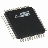
IC MCU 8K FLASH 24MHZ 44-TQFP
Manufacturer
Atmel
Series
89Sr
Datasheet
1.AT89S52-24AU.pdf
(38 pages)
Specifications of AT89S52-24AU
Core Processor
8051
Core Size
8-Bit
Speed
24MHz
Connectivity
UART/USART
Peripherals
WDT
Number Of I /o
32
Program Memory Size
8KB (8K x 8)
Program Memory Type
FLASH
Ram Size
256 x 8
Voltage - Supply (vcc/vdd)
4 V ~ 5.5 V
Oscillator Type
Internal
Operating Temperature
-40°C ~ 85°C
Package / Case
44-TQFP, 44-VQFP
Package
44TQFP
Device Core
8051
Family Name
89S
Maximum Speed
24 MHz
Operating Supply Voltage
5 V
Data Bus Width
8 Bit
Number Of Programmable I/os
32
Interface Type
UART
Number Of Timers
3
Processor Series
AT89x
Core
8051
Data Ram Size
256 B
Maximum Clock Frequency
24 MHz
Maximum Operating Temperature
+ 85 C
Mounting Style
SMD/SMT
3rd Party Development Tools
PK51, CA51, A51, ULINK2
Development Tools By Supplier
AT89ISP
Minimum Operating Temperature
- 40 C
No. Of I/o's
32
Ram Memory Size
256Byte
Cpu Speed
24MHz
No. Of Timers
3
Digital Ic Case Style
TQFP
Supply Voltage Range
4V To 5.5V
Rohs Compliant
Yes
Lead Free Status / RoHS Status
Lead free / RoHS Compliant
Eeprom Size
-
Data Converters
-
Lead Free Status / Rohs Status
Lead free / RoHS Compliant
Available stocks
Company
Part Number
Manufacturer
Quantity
Price
Company:

Part Number:
AT89S52-24AU
Manufacturer:
FEELING
Quantity:
43 000
Company:
Part Number:
AT89S52-24AU
Manufacturer:
ATMEL
Quantity:
930 880
Part Number:
AT89S52-24AU
Manufacturer:
ATMEL/爱特梅尔
Quantity:
20 000
Part Number:
AT89S52-24AUR
Manufacturer:
MICROCHIP/微芯
Quantity:
20 000


18. Programming the Flash – Parallel Mode
1919D–MICRO–6/08
The AT89S52 is shipped with the on-chip Flash memory array ready to be programmed. The
programming interface needs a high-voltage (12-volt) program enable signal and is compatible
with conventional third-party Flash or EPROM programmers.
The AT89S52 code memory array is programmed byte-by-byte.
Programming Algorithm: Before programming the AT89S52, the address, data, and control
signals should be set up according to the
22-1
Data Polling: The AT89S52 features Data Polling to indicate the end of a byte write cycle. Dur-
ing a write cycle, an attempted read of the last byte written will result in the complement of the
written data on P0.7. Once the write cycle has been completed, true data is valid on all outputs,
and the next cycle may begin. Data Polling may begin any time after a write cycle has been
initiated.
Ready/Busy: The progress of byte programming can also be monitored by the RDY/BSY output
signal. P3.0 is pulled low after ALE goes high during programming to indicate BUSY. P3.0 is
pulled high again when programming is done to indicate READY.
Program Verify: If lock bits LB1 and LB2 have not been programmed, the programmed code
data can be read back via the address and data lines for verification. The status of the individ-
ual lock bits can be verified directly by reading them back.
Reading the Signature Bytes: The signature bytes are read by the same procedure as a nor-
mal verification of locations 000H, 100H, and 200H, except that P3.6 and P3.7 must be pulled to
a logic low. The values returned are as follows.
Chip Erase: In the parallel programming mode, a chip erase operation is initiated by using the
proper combination of control signals and by pulsing ALE/PROG low for a duration of 200 ns -
500 ns.
In the serial programming mode, a chip erase operation is initiated by issuing the Chip Erase
instruction. In this mode, chip erase is self-timed and takes about 500 ms.
During chip erase, a serial read from any address location will return 00H at the data output.
1. Input the desired memory location on the address lines.
2. Input the appropriate data byte on the data lines.
3. Activate the correct combination of control signals.
4. Raise EA/V
5. Pulse ALE/PROG once to program a byte in the Flash array or the lock bits. The byte-
(000H) = 1EH indicates manufactured by Atmel
(100H) = 52H indicates AT89S52
(200H) = 06H
and
write cycle is self-timed and typically takes no more than 50 µs. Repeat steps 1
through 5, changing the address and data for the entire array or until the end of the
object file is reached.
Figure
22-2. To program the AT89S52, take the following steps:
PP
to 12V.
“Flash Programming Modes” (Table
AT89S52
22-1) and
Figure
21
Related parts for AT89S52-24AU
Image
Part Number
Description
Manufacturer
Datasheet
Request
R


Part Number:
Description:
IC MCU 8K FLASH 24MHZ 40-DIP
Manufacturer:
Atmel
Datasheet:

Part Number:
Description:
IC MCU 8K FLASH 24MHZ 44-PLCC
Manufacturer:
Atmel
Datasheet:

Part Number:
Description:
IC MCU 8K FLASH 24MHZ 44-TQFP
Manufacturer:
Atmel
Datasheet:
Part Number:
Description:
IC MCU 8K FLASH 24MHZ 44-PLCC
Manufacturer:
Atmel
Datasheet:
Part Number:
Description:
IC MCU 8K FLASH 24MHZ 44-PLCC
Manufacturer:
Atmel
Datasheet:
Part Number:
Description:
IC MCU 8K FLASH 24MHZ 40-DIP
Manufacturer:
Atmel
Datasheet:
Part Number:
Description:
IC MCU 8K FLASH 24MHZ 40-DIP
Manufacturer:
Atmel
Datasheet:
Part Number:
Description:
IC MCU 8K FLASH 24MHZ 44-TQFP
Manufacturer:
Atmel
Datasheet:

Part Number:
Description:
8-bit Microcontrollers - MCU Microcontroller
Manufacturer:
Atmel
Part Number:
Description:
8-bit Microcontrollers - MCU Microcontroller
Manufacturer:
Atmel
Part Number:
Description:
8-bit Microcontrollers - MCU Microcontroller
Manufacturer:
Atmel
Part Number:
Description:
8-bit Microcontrollers - MCU Microcontroller
Manufacturer:
Atmel
Part Number:
Description:
8-bit Microcontrollers - MCU Microcontroller
Manufacturer:
Atmel