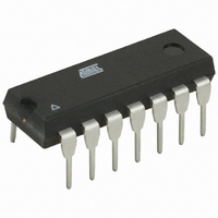
ATTINY24V-10PU Atmel, ATTINY24V-10PU Datasheet - Page 132

ATTINY24V-10PU
Manufacturer Part Number
ATTINY24V-10PU
Description
IC MCU AVR 2K FLASH 10MHZ 14-DIP
Manufacturer
Atmel
Series
AVR® ATtinyr
Specifications of ATTINY24V-10PU
Core Processor
AVR
Core Size
8-Bit
Speed
10MHz
Connectivity
USI
Peripherals
Brown-out Detect/Reset, POR, PWM, Temp Sensor, WDT
Number Of I /o
12
Program Memory Size
2KB (1K x 16)
Program Memory Type
FLASH
Eeprom Size
128 x 8
Ram Size
128 x 8
Voltage - Supply (vcc/vdd)
1.8 V ~ 5.5 V
Data Converters
A/D 8x10b
Oscillator Type
Internal
Operating Temperature
-40°C ~ 85°C
Package / Case
14-DIP (0.300", 7.62mm)
Processor Series
ATTINY2x
Core
AVR8
Data Bus Width
8 bit
Data Ram Size
128 B
Interface Type
SPI
Maximum Clock Frequency
10 MHz
Number Of Programmable I/os
12
Number Of Timers
2
Operating Supply Voltage
1.8 V to 5.5 V
Maximum Operating Temperature
+ 85 C
Mounting Style
Through Hole
Minimum Operating Temperature
- 40 C
On-chip Adc
8-ch x 10-bit
Cpu Family
ATtiny
Device Core
AVR
Device Core Size
8b
Frequency (max)
10MHz
Total Internal Ram Size
128Byte
# I/os (max)
12
Number Of Timers - General Purpose
2
Operating Supply Voltage (typ)
2.5/3.3/5V
Operating Supply Voltage (max)
5.5V
Operating Supply Voltage (min)
1.8V
Instruction Set Architecture
RISC
Operating Temp Range
-40C to 85C
Operating Temperature Classification
Industrial
Mounting
Through Hole
Pin Count
14
Package Type
PDIP
Package
14PDIP
Family Name
ATtiny
Maximum Speed
10 MHz
For Use With
ATSTK600-DIP40 - STK600 SOCKET/ADAPTER 40-PDIP770-1007 - ISP 4PORT ATMEL AVR MCU SPI/JTAGATAVRISP2 - PROGRAMMER AVR IN SYSTEMATSTK505 - ADAPTER KIT FOR 14PIN AVR MCU
Lead Free Status / RoHS Status
Lead free / RoHS Compliant
- Current page: 132 of 238
- Download datasheet (5Mb)
16. Analog to Digital Converter
16.1
16.2
132
Features
Overview
ATtiny24/44/84
•
•
•
•
•
•
•
•
•
•
•
•
•
•
•
•
•
The ATtiny24/44/84 features a 10-bit successive approximation ADC. The ADC is connected to
8-pin port A for external sources. In addition to external sources internal temperature sensor can
be measured by ADC. Analog Multiplexer allows eight single-ended channels or 12 differential
channels from Port A. The programmable gain stage provides ampification steps 0 dB (1x) and
26 dB (20x) for 12 differential ADC channels.
The ADC contains a Sample and Hold circuit which ensures that the input voltage to the ADC is
held at a constant level during conversion. A block diagram of the ADC is shown in
on page
Internal reference voltage of nominally 1.1V is provided On-chip. Alternatively, V
as reference voltage for single ended channels. There is also an option to use an external volt-
age reference and turn-off the internal voltage reference.
10-bit Resolution
1.0 LSB Integral Non-linearity
± 2 LSB Absolute Accuracy
13µs Conversion Time
15 kSPS at Maximum Resolution
Eight Multiplexed Single Ended Input Channels
Twelve Differential Input Channels with Selectable Gain (1x, 20x)
Temperature Sensor Input Channel
Optional Left Adjustment for ADC Result Readout
0 - V
1.1V ADC Reference Voltage
Free Running or Single Conversion Mode
ADC Start Conversion by Auto Triggering on Interrupt Sources
Interrupt on ADC Conversion Complete
Sleep Mode Noise Canceler
Unipolar / Bipolar Input Mode
Input Polarity Reversal Mode
CC
133.
ADC Input Voltage Range
CC
8006K–AVR–10/10
can be used
Figure 16-1
Related parts for ATTINY24V-10PU
Image
Part Number
Description
Manufacturer
Datasheet
Request
R

Part Number:
Description:
IC MCU AVR 2K FLASH 10MHZ 20-QFN
Manufacturer:
Atmel
Datasheet:

Part Number:
Description:
IC MCU AVR 2K FLASH 10MHZ 14SOIC
Manufacturer:
Atmel
Datasheet:

Part Number:
Description:
MCU AVR 2KB FLASH 10MHZ 14SOIC
Manufacturer:
Atmel
Datasheet:

Part Number:
Description:
MCU AVR 2KB FLASH 10MHZ 20QFN
Manufacturer:
Atmel
Datasheet:

Part Number:
Description:
8-bit Avr Microcontroller With 2/4/8k Bytes Insystem Programmable Flash
Manufacturer:
ATMEL Corporation
Datasheet:

Part Number:
Description:
8-bit Microcontrollers - MCU Microcontroller
Manufacturer:
Atmel

Part Number:
Description:
Manufacturer:
Atmel Corporation
Datasheet:

Part Number:
Description:
Manufacturer:
Atmel Corporation
Datasheet:

Part Number:
Description:
IC MCU AVR 2K FLASH 20MHZ 20-QFN
Manufacturer:
Atmel
Datasheet:

Part Number:
Description:
IC MCU AVR 2K FLASH 20MHZ 14SOIC
Manufacturer:
Atmel
Datasheet:

Part Number:
Description:
MCU AVR 2K FLASH 15MHZ 20-QFN
Manufacturer:
Atmel
Datasheet:

Part Number:
Description:
IC MCU AVR 2K FLASH 20MHZ 14-DIP
Manufacturer:
Atmel
Datasheet:


