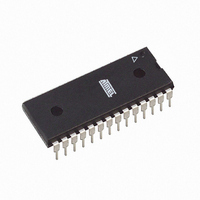
ATMEGA48A-PU Atmel, ATMEGA48A-PU Datasheet - Page 115

ATMEGA48A-PU
Manufacturer Part Number
ATMEGA48A-PU
Description
IC MCU AVR 4K FLASH 28PDIP
Manufacturer
Atmel
Series
AVR® ATmegar
Specifications of ATMEGA48A-PU
Core Processor
AVR
Core Size
8-Bit
Speed
20MHz
Connectivity
I²C, SPI, UART/USART
Peripherals
Brown-out Detect/Reset, POR, PWM, WDT
Number Of I /o
23
Program Memory Size
4KB (2K x 16)
Program Memory Type
FLASH
Eeprom Size
256 x 8
Ram Size
512 x 8
Voltage - Supply (vcc/vdd)
1.8 V ~ 5.5 V
Data Converters
A/D 6x10b
Oscillator Type
Internal
Operating Temperature
-40°C ~ 85°C
Package / Case
28-DIP (0.300", 7.62mm)
Controller Family/series
Atmega
No. Of I/o's
23
Eeprom Memory Size
256Byte
Ram Memory Size
512Byte
Cpu Speed
20MHz
Rohs Compliant
Yes
Lead Free Status / RoHS Status
Lead free / RoHS Compliant
- Current page: 115 of 566
- Download datasheet (23Mb)
15.2.1
8271C–AVR–08/10
Registers
Figure 15-1. 16-bit Timer/Counter Block Diagram
Note:
The Timer/Counter (TCNT1), Output Compare Registers (OCR1A/B), and Input Capture Regis-
ter (ICR1) are all 16-bit registers. Special procedures must be followed when accessing the 16-
bit registers. These procedures are described in the section
page
CPU access restrictions. Interrupt requests (abbreviated to Int.Req. in the figure) signals are all
visible in the Timer Interrupt Flag Register (TIFR1). All interrupts are individually masked with
the Timer Interrupt Mask Register (TIMSK1). TIFR1 and TIMSK1 are not shown in the figure.
The Timer/Counter can be clocked internally, via the prescaler, or by an external clock source on
the T1 pin. The Clock Select logic block controls which clock source and edge the Timer/Counter
uses to increment (or decrement) its value. The Timer/Counter is inactive when no clock source
is selected. The output from the Clock Select logic is referred to as the timer clock (clk
The double buffered Output Compare Registers (OCR1A/B) are compared with the Timer/Coun-
ter value at all time. The result of the compare can be used by the Waveform Generator to
generate a PWM or variable frequency output on the Output Compare pin (OC1A/B). See
ATmega48A/48PA/88A/88PA/168A/168PA/328/328
116. The Timer/Counter Control Registers (TCCR1A/B) are 8-bit registers and have no
1. Refer to
Timer/Counter1 pin placement and description.
Timer/Counter
Figure 1-1 on page
TCCRnA
OCRnA
OCRnB
TCNTn
ICRn
=
=
Direction
Count
Clear
2,
Table 13-3 on page 83
Control Logic
TOP
=
TCCRnB
Values
BOTTOM
Fixed
TOP
ICFn (Int.Req.)
(1)
clk
Detector
Edge
=
Tn
0
and
”Accessing 16-bit Registers” on
OCnA
(Int.Req.)
OCnB
(Int.Req.)
TOVn
(Int.Req.)
Clock Select
Generation
Generation
Table 13-9 on page 89
( From Prescaler )
Waveform
Waveform
Canceler
Detector
Noise
Edge
Comparator Ouput )
( From Analog
OCnA
OCnB
T
ICPn
1
Tn
).
for
”Out-
115
Related parts for ATMEGA48A-PU
Image
Part Number
Description
Manufacturer
Datasheet
Request
R

Part Number:
Description:
IC AVR MCU 4K 5V 20MHZ 32-TQFP
Manufacturer:
Atmel
Datasheet:

Part Number:
Description:
Manufacturer:
Atmel Corporation
Datasheet:

Part Number:
Description:
Manufacturer:
Atmel Corporation
Datasheet:

Part Number:
Description:
IC AVR MCU 4K 20MHZ 5V 32TQFP
Manufacturer:
Atmel
Datasheet:

Part Number:
Description:
IC AVR MCU 4K 20MHZ 5V 28DIP
Manufacturer:
Atmel
Datasheet:

Part Number:
Description:
IC AVR MCU 4K 20MHZ 5V 32-QFN
Manufacturer:
Atmel
Datasheet:

Part Number:
Description:
IC AVR MCU 4K 5V 20MHZ 32-TQFP
Manufacturer:
Atmel
Datasheet:

Part Number:
Description:
IC AVR MCU 4K 5V 20MHZ 32-QFN
Manufacturer:
Atmel
Datasheet:

Part Number:
Description:
IC AVR MCU 4K 5V 20MHZ 32-QFN
Manufacturer:
Atmel
Datasheet:

Part Number:
Description:
IC AVR MCU 4K 5V 20MHZ 28-DIP
Manufacturer:
Atmel
Datasheet:

Part Number:
Description:
IC AVR MCU 4K 5V 20MHZ 28-DIP
Manufacturer:
Atmel
Datasheet:

Part Number:
Description:
IC AVR MCU 4K FLASH 20MHZ 28QFN
Manufacturer:
Atmel
Datasheet:


