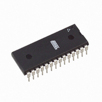
ATMEGA48A-PU Atmel, ATMEGA48A-PU Datasheet - Page 299

ATMEGA48A-PU
Manufacturer Part Number
ATMEGA48A-PU
Description
IC MCU AVR 4K FLASH 28PDIP
Manufacturer
Atmel
Series
AVR® ATmegar
Specifications of ATMEGA48A-PU
Core Processor
AVR
Core Size
8-Bit
Speed
20MHz
Connectivity
I²C, SPI, UART/USART
Peripherals
Brown-out Detect/Reset, POR, PWM, WDT
Number Of I /o
23
Program Memory Size
4KB (2K x 16)
Program Memory Type
FLASH
Eeprom Size
256 x 8
Ram Size
512 x 8
Voltage - Supply (vcc/vdd)
1.8 V ~ 5.5 V
Data Converters
A/D 6x10b
Oscillator Type
Internal
Operating Temperature
-40°C ~ 85°C
Package / Case
28-DIP (0.300", 7.62mm)
Controller Family/series
Atmega
No. Of I/o's
23
Eeprom Memory Size
256Byte
Ram Memory Size
512Byte
Cpu Speed
20MHz
Rohs Compliant
Yes
Lead Free Status / RoHS Status
Lead free / RoHS Compliant
- Current page: 299 of 566
- Download datasheet (23Mb)
8271C–AVR–08/10
Table 27-7.
Notes:
Table 27-8.
Notes:
ATmega48A/48PA/88A/88PA/168A/168PA/328/328
High Fuse Byte
WDTON
EESAVE
BODLEVEL2
BODLEVEL1
BODLEVEL0
High Fuse Byte
RSTDISBL
DWEN
SPIEN
WDTON
EESAVE
BOOTSZ1
BOOTSZ0
BOOTRST
(2)
1. See
2. The SPIEN Fuse is not accessible in serial programming mode.
3. See
4. See
1. See
2. The SPIEN Fuse is not accessible in serial programming mode.
3. See
4. The default value of BOOTSZ[1:0] results in maximum Boot Size. See
(3)
(3)
(1)
page
(4)
(4)
(4)
Fuse High Byte for ATmega48A/48PA/88A/88PA/168A/168PA (Continued)
Fuse High Byte for ATmega328/328P
”Alternate Functions of Port C” on page 86
”WDTCSR – Watchdog Timer Control Register” on page 55
Table 28-13 on page 323
”Alternate Functions of Port C” on page 86
”WDTCSR – Watchdog Timer Control Register” on page 55
303.
Bit No
Bit No
4
3
2
1
0
7
6
5
4
3
2
1
0
Description
Watchdog Timer Always On
EEPROM memory is
preserved through the Chip
Erase
Brown-out Detector trigger
level
Brown-out Detector trigger
level
Brown-out Detector trigger
level
Description
External Reset Disable
debugWIRE Enable
Enable Serial Program and
Data Downloading
Watchdog Timer Always On
EEPROM memory is
preserved through the Chip
Erase
Select Boot Size
(see
Table 26-7 on page
Table 26-10 on page 292
Table 26-13 on page 293
for details)
Select Boot Size
(see
Table 26-7 on page
Table 26-10 on page 292
Table 26-13 on page 293
for details)
Select Reset Vector
for BODLEVEL Fuse decoding.
for description of RSTDISBL Fuse.
for description of RSTDISBL Fuse.
291,
291,
and
and
Default Value
1 (unprogrammed)
1 (unprogrammed), EEPROM
not reserved
1 (unprogrammed)
1 (unprogrammed)
1 (unprogrammed)
Default Value
1 (unprogrammed)
1 (unprogrammed)
0 (programmed, SPI
programming enabled)
1 (unprogrammed)
1 (unprogrammed), EEPROM
not reserved
0 (programmed)
0 (programmed)
1 (unprogrammed)
for details.
for details.
”Pin Name Mapping” on
(4)
(4)
299
Related parts for ATMEGA48A-PU
Image
Part Number
Description
Manufacturer
Datasheet
Request
R

Part Number:
Description:
IC AVR MCU 4K 5V 20MHZ 32-TQFP
Manufacturer:
Atmel
Datasheet:

Part Number:
Description:
Manufacturer:
Atmel Corporation
Datasheet:

Part Number:
Description:
Manufacturer:
Atmel Corporation
Datasheet:

Part Number:
Description:
IC AVR MCU 4K 20MHZ 5V 32TQFP
Manufacturer:
Atmel
Datasheet:

Part Number:
Description:
IC AVR MCU 4K 20MHZ 5V 28DIP
Manufacturer:
Atmel
Datasheet:

Part Number:
Description:
IC AVR MCU 4K 20MHZ 5V 32-QFN
Manufacturer:
Atmel
Datasheet:

Part Number:
Description:
IC AVR MCU 4K 5V 20MHZ 32-TQFP
Manufacturer:
Atmel
Datasheet:

Part Number:
Description:
IC AVR MCU 4K 5V 20MHZ 32-QFN
Manufacturer:
Atmel
Datasheet:

Part Number:
Description:
IC AVR MCU 4K 5V 20MHZ 32-QFN
Manufacturer:
Atmel
Datasheet:

Part Number:
Description:
IC AVR MCU 4K 5V 20MHZ 28-DIP
Manufacturer:
Atmel
Datasheet:

Part Number:
Description:
IC AVR MCU 4K 5V 20MHZ 28-DIP
Manufacturer:
Atmel
Datasheet:

Part Number:
Description:
IC AVR MCU 4K FLASH 20MHZ 28QFN
Manufacturer:
Atmel
Datasheet:


