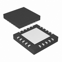
PIC18LF13K50-I/MQ Microchip Technology, PIC18LF13K50-I/MQ Datasheet - Page 94

PIC18LF13K50-I/MQ
Manufacturer Part Number
PIC18LF13K50-I/MQ
Description
IC PIC MCU FLASH 512KX8 20-QFN
Manufacturer
Microchip Technology
Series
PIC® XLP™ 18Fr
Datasheets
1.PIC18F13K50-ISS.pdf
(420 pages)
2.PIC18F13K50-ISS.pdf
(40 pages)
3.PIC18F13K50-ISS.pdf
(10 pages)
4.PIC18F13K50-ISS.pdf
(2 pages)
5.PIC18F14K50-IP.pdf
(422 pages)
Specifications of PIC18LF13K50-I/MQ
Program Memory Type
FLASH
Program Memory Size
8KB (4K x 16)
Package / Case
20-QFN
Core Processor
PIC
Core Size
8-Bit
Speed
48MHz
Connectivity
I²C, SPI, UART/USART, USB
Peripherals
Brown-out Detect/Reset, POR, PWM, WDT
Number Of I /o
14
Eeprom Size
256 x 8
Ram Size
512 x 8
Voltage - Supply (vcc/vdd)
1.8 V ~ 3.6 V
Data Converters
A/D 11x10b
Oscillator Type
Internal
Operating Temperature
-40°C ~ 85°C
Processor Series
PIC18LF
Core
PIC
Data Bus Width
8 bit
Data Ram Size
512 B
Interface Type
EUSART/I2C/MSSP/SPI/USB
Maximum Clock Frequency
48 MHz
Number Of Programmable I/os
15
Number Of Timers
4
Operating Supply Voltage
1.8 V to 3.6 V
Maximum Operating Temperature
+ 85 C
Mounting Style
SMD/SMT
3rd Party Development Tools
52715-96, 52716-328, 52717-734, 52712-325, EWPIC18
Development Tools By Supplier
PG164130, DV164035, DV244005, DV164005, DM164127, DV164126
Minimum Operating Temperature
- 40 C
On-chip Adc
11-ch x 10-bit
Controller Family/series
PIC18
No. Of I/o's
15
Eeprom Memory Size
256Byte
Ram Memory Size
512Byte
Cpu Speed
48MHz
No. Of Timers
4
Lead Free Status / RoHS Status
Lead free / RoHS Compliant
Lead Free Status / RoHS Status
Lead free / RoHS Compliant, Lead free / RoHS Compliant
Available stocks
Company
Part Number
Manufacturer
Quantity
Price
Company:
Part Number:
PIC18LF13K50-I/MQ
Manufacturer:
MICROCHIP
Quantity:
2 400
- PIC18F13K50-ISS PDF datasheet
- PIC18F13K50-ISS PDF datasheet #2
- PIC18F13K50-ISS PDF datasheet #3
- PIC18F13K50-ISS PDF datasheet #4
- PIC18F14K50-IP PDF datasheet #5
- Current page: 94 of 420
- Download datasheet (4Mb)
PIC18F/LF1XK50
9.3
PORTC is an 8-bit wide, bidirectional port. The corre-
sponding data direction register is TRISC. Setting a
TRISC bit (= 1) will make the corresponding PORTC
pin an input (i.e., disable the output driver). Clearing a
TRISC bit (= 0) will make the corresponding PORTC
pin an output (i.e., enable the output driver and put the
contents of the output latch on the selected pin).
The PORTC Data Latch register (LATC) is also
memory mapped. Read-modify-write operations on the
LATC register read and write the latched output value
for PORTC.
REGISTER 9-11:
REGISTER 9-12:
DS41350E-page 94
bit 7
Legend:
R = Readable bit
-n = Value at POR
bit 7-0
bit 7
Legend:
R = Readable bit
-n = Value at POR
bit 7-0
TRISC7
R/W-1
R/W-x
RC7
PORTC, TRISC and LATC
Registers
RC<7:0>: PORTC I/O Pin bit
1 = Port pin is > V
0 = Port pin is < V
TRISC<7:0>: PORTC Tri-State Control bit
1 = PORTC pin configured as an input (tri-stated)
0 = PORTC pin configured as an output
TRISC6
R/W-x
R/W-1
RC6
PORTC: PORTC REGISTER
TRISC: PORTC TRI-STATE REGISTER
W = Writable bit
W = Writable bit
‘1’ = Bit is set
‘1’ = Bit is set
TRISC5
R/W-x
IH
IL
R/W-1
RC5
TRISC4
R/W-1
R/W-x
RC4
Preliminary
U = Unimplemented bit, read as ‘0’
‘0’ = Bit is cleared
U = Unimplemented bit, read as ‘0’
‘0’ = Bit is cleared
TRISC3
R/W-x
R/W-1
All the pins on PORTC are implemented with Schmitt
Trigger input buffer. Each pin is individually configu-
rable as an input or output.
EXAMPLE 9-3:
RC3
CLRF
CLRF
MOVLW
MOVWF
Note:
PORTC
LATC
0CFh
TRISC
On a Power-on Reset, RC<7:6> and
RC<3:0> are configured as analog inputs
and read as ‘0’.
TRISC2
R/W-1
R/W-x
RC2
; Initialize PORTC by
; clearing output
; data latches
; Alternate method
; to clear output
; data latches
; Value used to
; initialize data
; direction
; Set RC<3:0> as inputs
; RC<5:4> as outputs
; RC<7:6> as inputs
INITIALIZING PORTC
2010 Microchip Technology Inc.
x = Bit is unknown
x = Bit is unknown
TRISC1
R/W-x
R/W-1
RC1
TRISC0
R/W-1
R/W-x
RC0
bit 0
bit 0
Related parts for PIC18LF13K50-I/MQ
Image
Part Number
Description
Manufacturer
Datasheet
Request
R

Part Number:
Description:
Manufacturer:
Microchip Technology Inc.
Datasheet:

Part Number:
Description:
Manufacturer:
Microchip Technology Inc.
Datasheet:

Part Number:
Description:
Manufacturer:
Microchip Technology Inc.
Datasheet:

Part Number:
Description:
Manufacturer:
Microchip Technology Inc.
Datasheet:

Part Number:
Description:
Manufacturer:
Microchip Technology Inc.
Datasheet:

Part Number:
Description:
Manufacturer:
Microchip Technology Inc.
Datasheet:

Part Number:
Description:
Manufacturer:
Microchip Technology Inc.
Datasheet:

Part Number:
Description:
Manufacturer:
Microchip Technology Inc.
Datasheet:


