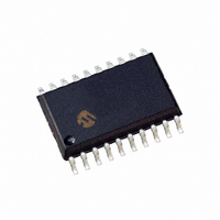
DSPIC33FJ12MC201-I/SO Microchip Technology, DSPIC33FJ12MC201-I/SO Datasheet - Page 206

DSPIC33FJ12MC201-I/SO
Manufacturer Part Number
DSPIC33FJ12MC201-I/SO
Description
IC DSPIC MCU/DSP 12K 20SOIC
Manufacturer
Microchip Technology
Series
dsPIC™ 33Fr
Datasheets
1.PIC24HJ12GP201-ISO.pdf
(84 pages)
2.DSPIC33FJ12MC201-ISO.pdf
(288 pages)
3.DSPIC33FJ12MC201-ISO.pdf
(14 pages)
4.DSPIC33FJ12MC201-IP.pdf
(284 pages)
Specifications of DSPIC33FJ12MC201-I/SO
Program Memory Type
FLASH
Program Memory Size
12KB (12K x 8)
Package / Case
20-SOIC (7.5mm Width)
Core Processor
dsPIC
Core Size
16-Bit
Speed
40 MIPs
Connectivity
I²C, IrDA, SPI, UART/USART
Peripherals
Brown-out Detect/Reset, Motor Control PWM, QEI, POR, PWM, WDT
Number Of I /o
15
Ram Size
1K x 8
Voltage - Supply (vcc/vdd)
3 V ~ 3.6 V
Data Converters
A/D 4x10b
Oscillator Type
Internal
Operating Temperature
-40°C ~ 85°C
Product
DSCs
Data Bus Width
16 bit
Processor Series
DSPIC33F
Core
dsPIC
Maximum Clock Frequency
40 MHz
Number Of Programmable I/os
15
Data Ram Size
1 KB
Maximum Operating Temperature
+ 85 C
Mounting Style
SMD/SMT
3rd Party Development Tools
52713-733, 52714-737, 53276-922, EWDSPIC
Development Tools By Supplier
PG164130, DV164035, DV244005, DV164005, PG164120, DM240001, DV164033
Minimum Operating Temperature
- 40 C
Lead Free Status / RoHS Status
Lead free / RoHS Compliant
For Use With
DV164033 - KIT START EXPLORER 16 MPLAB ICD2DM240001 - BOARD DEMO PIC24/DSPIC33/PIC32
Eeprom Size
-
Lead Free Status / Rohs Status
Lead free / RoHS Compliant
- PIC24HJ12GP201-ISO PDF datasheet
- DSPIC33FJ12MC201-ISO PDF datasheet #2
- DSPIC33FJ12MC201-ISO PDF datasheet #3
- DSPIC33FJ12MC201-IP PDF datasheet #4
- Current page: 206 of 288
- Download datasheet (5Mb)
dsPIC33FJ12MC201/202
TABLE 21-2:
DS70265D-page 204
WDTPOST<3:0>
POSCMD<1:0>
FPWRT<2:0>
WDTPRE
FWDTEN
PWMPIN
Bit Field
JTAGEN
WINDIS
ALTI2C
HPOL
LPOL
dsPIC33F CONFIGURATION BITS DESCRIPTION (CONTINUED)
Register
FWDT
FWDT
FWDT
FWDT
FOSC
FPOR
FPOR
FPOR
FPOR
FPOR
FICD
Primary Oscillator Mode Select bits
11 = Primary oscillator disabled
10 = HS Crystal Oscillator mode
01 = XT Crystal Oscillator mode
00 = EC (External Clock) mode
Watchdog Timer Enable bit
1 = Watchdog Timer always enabled (LPRC oscillator cannot be disabled.
0 = Watchdog Timer enabled/disabled by user software (LPRC can be
Watchdog Timer Window Enable bit
1 = Watchdog Timer in Non-Window mode
0 = Watchdog Timer in Window mode
Watchdog Timer Prescaler bit
1 = 1:128
0 = 1:32
Watchdog Timer Postscaler bits
1111 = 1:32,768
1110 = 1:16,384
0001 = 1:2
0000 = 1:1
Motor Control PWM Module Pin Mode bit
1 = PWM module pins controlled by PORT register at device Reset
0 = PWM module pins controlled by PWM module at device Reset
Motor Control PWM High Side Polarity bit
1 = PWM module high side output pins have active-high output polarity
0 = PWM module high side output pins have active-low output polarity
Motor Control PWM Low Side Polarity bit
1 = PWM module low side output pins have active-high output polarity
0 = PWM module low side output pins have active-low output polarity
Power-on Reset Timer Value Select bits
111 = PWRT = 128 ms
110 = PWRT = 64 ms
101 = PWRT = 32 ms
100 = PWRT = 16 ms
011 = PWRT = 8 ms
010 = PWRT = 4 ms
001 = PWRT = 2 ms
000 = PWRT = Disabled
Alternate I
1 = I
0 = I
JTAG Enable bit
1 = JTAG enabled
0 = JTAG disabled
.
.
.
Clearing the SWDTEN bit in the RCON register will have no effect.)
disabled by clearing the SWDTEN bit in the RCON register)
(tri-stated)
(configured as output pins)
2
2
Preliminary
C mapped to SDA1/SCL1 pins
C mapped to ASDA1/ASCL1 pins
2
C pins
Description
© 2009 Microchip Technology Inc.
Related parts for DSPIC33FJ12MC201-I/SO
Image
Part Number
Description
Manufacturer
Datasheet
Request
R

Part Number:
Description:
IC, DSC, 16BIT, 12KB, 40MHZ, 3.6V, DIP28
Manufacturer:
Microchip Technology
Datasheet:

Part Number:
Description:
Manufacturer:
Microchip Technology Inc.
Datasheet:

Part Number:
Description:
Manufacturer:
Microchip Technology Inc.
Datasheet:

Part Number:
Description:
Manufacturer:
Microchip Technology Inc.
Datasheet:

Part Number:
Description:
Manufacturer:
Microchip Technology Inc.
Datasheet:

Part Number:
Description:
Manufacturer:
Microchip Technology Inc.
Datasheet:

Part Number:
Description:
Manufacturer:
Microchip Technology Inc.
Datasheet:

Part Number:
Description:
Manufacturer:
Microchip Technology Inc.
Datasheet:

Part Number:
Description:
Manufacturer:
Microchip Technology Inc.
Datasheet:


