PIC18F47J13-I/PT Microchip Technology, PIC18F47J13-I/PT Datasheet - Page 183
PIC18F47J13-I/PT
Manufacturer Part Number
PIC18F47J13-I/PT
Description
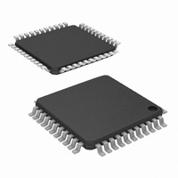
IC PIC MCU 128KB FLASH 44TQFP
Manufacturer
Microchip Technology
Series
PIC® XLP™ 18Fr
Datasheets
1.PIC18LF24J10-ISS.pdf
(32 pages)
2.PIC18F26J13-ISS.pdf
(496 pages)
3.PIC18F26J13-ISS.pdf
(558 pages)
4.PIC18F26J13-ISS.pdf
(12 pages)
Specifications of PIC18F47J13-I/PT
Program Memory Type
FLASH
Program Memory Size
128KB (64K x 16)
Package / Case
*
Core Processor
PIC
Core Size
8-Bit
Speed
48MHz
Connectivity
I²C, LIN, SPI, UART/USART
Peripherals
Brown-out Detect/Reset, POR, PWM, WDT
Number Of I /o
34
Ram Size
3.8K x 8
Voltage - Supply (vcc/vdd)
2.15 V ~ 3.6 V
Data Converters
A/D 13x10b/12b
Oscillator Type
Internal
Operating Temperature
-40°C ~ 85°C
Processor Series
PIC18F
Core
PIC
Data Bus Width
8 bit
Data Ram Size
4 KB
Interface Type
I2C, SPI, EUSART
Maximum Clock Frequency
48 MHz
Number Of Programmable I/os
25
Number Of Timers
8
Operating Supply Voltage
2 V to 3.6 V
Maximum Operating Temperature
+ 85 C
Mounting Style
SMD/SMT
3rd Party Development Tools
52715-96, 52716-328, 52717-734, 52712-325, EWPIC18
Development Tools By Supplier
DM164128, DM180021, DM183026-2, DV164131, MA180030, DM183022, DM183032, DV164136, MA180024
Minimum Operating Temperature
- 40 C
On-chip Adc
12 bit, 13 Channel
Controller Family/series
PIC18
Cpu Speed
48MHz
Embedded Interface Type
I2C, SPI, USART
Digital Ic Case Style
TQFP
Supply Voltage Range
1.8V To 5.5V
Rohs Compliant
Yes
Lead Free Status / RoHS Status
Lead free / RoHS Compliant
For Use With
MA180030 - BOARD DEMO PIC18F47J13 FS USBMA180029 - BOARD DEMO PIC18F47J53 FS USB
Eeprom Size
-
Lead Free Status / Rohs Status
Lead free / RoHS Compliant
Available stocks
Company
Part Number
Manufacturer
Quantity
Price
Company:

Part Number:
PIC18F47J13-I/PT
Manufacturer:
Microchip Technology
Quantity:
10 000


REGISTER 11-4:
2010 Microchip Technology Inc.
bit 7
Legend:
R = Readable bit
-n = Value at POR
bit 7-6
bit 5-2
bit 1-0
Note 1:
WAITB1
R/W-0
2:
(2)
This register is only available on 44-pin devices.
WAITBx and WAITEx bits are ignored whenever WAITM<3:0> = 0000.
WAITB<1:0>: Data Setup to Read/Write Wait State Configuration bits
11 = Data Wait of 4 T
10 = Data Wait of 3 T
01 = Data Wait of 2 T
00 = Data Wait of 1 T
WAITM<3:0>: Read to Byte Enable Strobe Wait State Configuration bits
1111 = Wait of additional 15 T
.
.
.
0001 = Wait of additional 1 T
0000 = No additional Wait cycles (operation forced into one T
WAITE<1:0>: Data Hold After Strobe Wait State Configuration bits
11 = Wait of 4 T
10 = Wait of 3 T
01 = Wait of 2 T
00 = Wait of 1 T
WAITB0
R/W-0
PMMODEL: PARALLEL PORT MODE REGISTER LOW BYTE (BANKED F5Ch)
(2)
W = Writable bit
‘1’ = Bit is set
CY
CY
CY
CY
WAITM3
R/W-0
CY
CY
CY
CY
; multiplexed address phase of 4 T
; multiplexed address phase of 3 T
; multiplexed address phase of 2 T
; multiplexed address phase of 1 T
CY
CY
WAITM2
R/W-0
Preliminary
U = Unimplemented bit, read as ‘0’
‘0’ = Bit is cleared
PIC18F47J13 FAMILY
WAITM1
R/W-0
CY
CY
CY
CY
WAITM0
CY
R/W-0
)
(2)
(2)
x = Bit is unknown
WAITE1
R/W-0
(2)
DS39974A-page 183
WAITE0
R/W-0
bit 0
(2)
(1)
Related parts for PIC18F47J13-I/PT
Image
Part Number
Description
Manufacturer
Datasheet
Request
R

Part Number:
Description:
Manufacturer:
Microchip Technology Inc.
Datasheet:
Part Number:
Description:
Manufacturer:
Microchip Technology Inc.
Datasheet:
Part Number:
Description:
Manufacturer:
Microchip Technology Inc.
Datasheet:
Part Number:
Description:
Manufacturer:
Microchip Technology Inc.
Datasheet:
Part Number:
Description:
Manufacturer:
Microchip Technology Inc.
Datasheet:
Part Number:
Description:
Manufacturer:
Microchip Technology Inc.
Datasheet:
Part Number:
Description:
Manufacturer:
Microchip Technology Inc.
Datasheet:
Part Number:
Description:
Manufacturer:
Microchip Technology Inc.
Datasheet: