DSPIC33FJ128GP706A-I/MR Microchip Technology, DSPIC33FJ128GP706A-I/MR Datasheet - Page 14
DSPIC33FJ128GP706A-I/MR
Manufacturer Part Number
DSPIC33FJ128GP706A-I/MR
Description
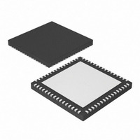
IC DSPIC MCU/DSP 128K 64-QFN
Manufacturer
Microchip Technology
Series
dsPIC™ 33Fr
Datasheets
1.MCP3909T-ISS.pdf
(104 pages)
2.DSPIC33FJ12GP201-ISO.pdf
(90 pages)
3.DSPIC33FJ64GP206-IPT.pdf
(28 pages)
4.DSPIC33FJ64GP206A-IMR.pdf
(338 pages)
Specifications of DSPIC33FJ128GP706A-I/MR
Core Processor
dsPIC
Core Size
16-Bit
Speed
40 MIPs
Connectivity
CAN, I²C, IrDA, LIN, SPI, UART/USART
Peripherals
AC'97, Brown-out Detect/Reset, DMA, I²S, POR, PWM, WDT
Number Of I /o
53
Program Memory Size
128KB (128K x 8)
Program Memory Type
FLASH
Ram Size
16K x 8
Voltage - Supply (vcc/vdd)
3 V ~ 3.6 V
Data Converters
A/D 18x10b/12b
Oscillator Type
Internal
Operating Temperature
-40°C ~ 85°C
Package / Case
64-VFQFN, Exposed Pad
Product
DSCs
Processor Series
DSPIC33F
Core
dsPIC
3rd Party Development Tools
52713-733, 52714-737, 53276-922, EWDSPIC
Development Tools By Supplier
PG164130, DV164035, DV244005, DV164005, PG164120, DM240001, DV164033
Core Frequency
40MHz
Core Supply Voltage
3.3V
Embedded Interface Type
I2C, SPI, UART
No. Of I/o's
53
Flash Memory Size
128KB
Supply Voltage Range
3V To 3.6V
Rohs Compliant
No
Lead Free Status / RoHS Status
Lead free / RoHS Compliant
Eeprom Size
-
Lead Free Status / Rohs Status
Lead free / RoHS Compliant


26. Module: Interrupt Controller
DS80446D-page 14
If a clock failure occurs when the device is in Idle
mode, the oscillator failure trap does not vector to
the Trap Service Routine. Instead, the device will
simply wake-up from Idle mode and continue code
execution if the Fail-Safe Clock Monitor (FSCM) is
enabled.
Work around
Whenever the device wakes up from Idle
(assuming the FSCM is enabled) the user software
should check the state of the OSCFAIL bit
(INTCON1<1>) to determine whether a clock
failure occurred, and then perform the appropriate
clock switch operation. Regardless, the Trap
Service Routine must be included in the user
application.
Affected Silicon Revisions
A2
X
A3
X
A4
X
27. Module: Internal Voltage Regulator
28. Module: ECAN
If a MCLR Reset pulse causes the device to wake-
up from Sleep mode, the device wakes up without
waiting for the on-chip voltage regulator to power-
up. This will subsequently result in a Brown-out
Reset (BOR).
Work around
None.
Affected Silicon Revisions
The C1RXOVF2 and C2RXOVF2 registers are
non-functional. They are always read back as
0x0000, even when a receive overflow has
occurred.
Work around
None.
Affected Silicon Revisions
A2
A2
X
X
A3
A3
X
X
A4
A4
X
X
© 2010 Microchip Technology Inc.
Related parts for DSPIC33FJ128GP706A-I/MR
Image
Part Number
Description
Manufacturer
Datasheet
Request
R

Part Number:
Description:
Manufacturer:
Microchip Technology Inc.
Datasheet:
Part Number:
Description:
Manufacturer:
Microchip Technology Inc.
Datasheet:
Part Number:
Description:
Manufacturer:
Microchip Technology Inc.
Datasheet:
Part Number:
Description:
Manufacturer:
Microchip Technology Inc.
Datasheet:
Part Number:
Description:
Manufacturer:
Microchip Technology Inc.
Datasheet:
Part Number:
Description:
Manufacturer:
Microchip Technology Inc.
Datasheet:
Part Number:
Description:
Manufacturer:
Microchip Technology Inc.
Datasheet:
Part Number:
Description:
Manufacturer:
Microchip Technology Inc.
Datasheet: