DSPIC33FJ128GP706A-I/MR Microchip Technology, DSPIC33FJ128GP706A-I/MR Datasheet - Page 18
DSPIC33FJ128GP706A-I/MR
Manufacturer Part Number
DSPIC33FJ128GP706A-I/MR
Description
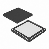
IC DSPIC MCU/DSP 128K 64-QFN
Manufacturer
Microchip Technology
Series
dsPIC™ 33Fr
Datasheets
1.MCP3909T-ISS.pdf
(104 pages)
2.DSPIC33FJ12GP201-ISO.pdf
(90 pages)
3.DSPIC33FJ64GP206-IPT.pdf
(28 pages)
4.DSPIC33FJ64GP206A-IMR.pdf
(338 pages)
Specifications of DSPIC33FJ128GP706A-I/MR
Core Processor
dsPIC
Core Size
16-Bit
Speed
40 MIPs
Connectivity
CAN, I²C, IrDA, LIN, SPI, UART/USART
Peripherals
AC'97, Brown-out Detect/Reset, DMA, I²S, POR, PWM, WDT
Number Of I /o
53
Program Memory Size
128KB (128K x 8)
Program Memory Type
FLASH
Ram Size
16K x 8
Voltage - Supply (vcc/vdd)
3 V ~ 3.6 V
Data Converters
A/D 18x10b/12b
Oscillator Type
Internal
Operating Temperature
-40°C ~ 85°C
Package / Case
64-VFQFN, Exposed Pad
Product
DSCs
Processor Series
DSPIC33F
Core
dsPIC
3rd Party Development Tools
52713-733, 52714-737, 53276-922, EWDSPIC
Development Tools By Supplier
PG164130, DV164035, DV244005, DV164005, PG164120, DM240001, DV164033
Core Frequency
40MHz
Core Supply Voltage
3.3V
Embedded Interface Type
I2C, SPI, UART
No. Of I/o's
53
Flash Memory Size
128KB
Supply Voltage Range
3V To 3.6V
Rohs Compliant
No
Lead Free Status / RoHS Status
Lead free / RoHS Compliant
Eeprom Size
-
Lead Free Status / Rohs Status
Lead free / RoHS Compliant


38. Module: DMA
39. Module: DMA
DS80446D-page 18
When the DMA channel is configured for NULL
Data
(DMAxCON<11> = 1), it does not execute a NULL
(all zeros) write to the peripheral address.
Work around
Use two DMA channels to receive data from the
peripheral
configured to transfer data from the peripheral to
DMA RAM, while another channel must be
configured to transfer dummy data from the DMA
RAM to the peripheral. Both channels must be
setup for the same DMA request.
Affected Silicon Revisions
A low priority DMA channel request can be
preempted by a higher priority DMA channel
request. For example, if DMA Channel 0 has a
higher priority than DMA Channel 1. A request to
DMA channel 1 will be pending while DMA
Channel 0 is processing its request. If DMA
Channel 1 receives another request while it is in a
pending request state, the DMA module does not
generate a DMA error trap event.
Work around
None. Using higher priority DMA channels for
servicing sources of frequent requests significantly
reduces the possibility of the condition described
above occurring, but does not completely
eliminate it.
Affected Silicon Revisions
A2
A2
X
X
A3
A3
X
X
module.
Peripheral
A4
A4
X
X
One
channel
Write
must
mode
be
40. Module: DMA
41. Module: CPU
When the DMA channel is configured for One Shot
mode with NULL write enabled, the channel will
write an extra NULL to the peripheral register after
completing the last transfer. In the case of the SPI
module and the SPIxBUF register, this would
cause the SPI module to perform an extra receive
operation.
Work around
None. In the case of using DMA NULL write with
the SPI module, perform a dummy read of the
SPIxBUF register after the DMA transfer is
completed to clear the SPIRBF flag and prevent an
un-expected overflow condition on the next SPI
receive operation.
Affected Silicon Revisions
Any instruction executed inside a REPEAT loop,
which produces a Read-After-Write stall condition,
results in the instruction being executed fewer
times than was intended.
An example of such code is:
repeat #0xf
inc [w1],[++w1]
Work around
Avoid repeating an instruction that creates a stall
using a REPEAT instruction. Instead, use a
software loop using conditional branches.
Affected Silicon Revisions
A2
A2
X
X
A3
A3
X
X
A4
A4
X
X
© 2010 Microchip Technology Inc.
Related parts for DSPIC33FJ128GP706A-I/MR
Image
Part Number
Description
Manufacturer
Datasheet
Request
R

Part Number:
Description:
Manufacturer:
Microchip Technology Inc.
Datasheet:
Part Number:
Description:
Manufacturer:
Microchip Technology Inc.
Datasheet:
Part Number:
Description:
Manufacturer:
Microchip Technology Inc.
Datasheet:
Part Number:
Description:
Manufacturer:
Microchip Technology Inc.
Datasheet:
Part Number:
Description:
Manufacturer:
Microchip Technology Inc.
Datasheet:
Part Number:
Description:
Manufacturer:
Microchip Technology Inc.
Datasheet:
Part Number:
Description:
Manufacturer:
Microchip Technology Inc.
Datasheet:
Part Number:
Description:
Manufacturer:
Microchip Technology Inc.
Datasheet: