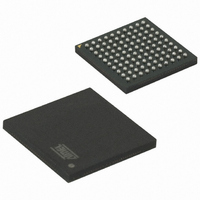
ATMEGA2560V-8CU Atmel, ATMEGA2560V-8CU Datasheet - Page 173

ATMEGA2560V-8CU
Manufacturer Part Number
ATMEGA2560V-8CU
Description
IC MCU AVR 256K FLASH 100-CBGA
Manufacturer
Atmel
Series
AVR® ATmegar
Specifications of ATMEGA2560V-8CU
Core Processor
AVR
Core Size
8-Bit
Speed
8MHz
Connectivity
EBI/EMI, I²C, SPI, UART/USART
Peripherals
Brown-out Detect/Reset, POR, PWM, WDT
Number Of I /o
86
Program Memory Size
256KB (128K x 16)
Program Memory Type
FLASH
Eeprom Size
4K x 8
Ram Size
8K x 8
Voltage - Supply (vcc/vdd)
1.8 V ~ 5.5 V
Data Converters
A/D 16x10b
Oscillator Type
Internal
Operating Temperature
-40°C ~ 85°C
Package / Case
100-TFBGA
Processor Series
ATMEGA256x
Core
AVR8
Data Bus Width
8 bit
Data Ram Size
8 KB
Interface Type
2-Wire, SPI, USART
Maximum Clock Frequency
8 MHz
Number Of Programmable I/os
86
Number Of Timers
6
Maximum Operating Temperature
+ 85 C
Mounting Style
SMD/SMT
3rd Party Development Tools
EWAVR, EWAVR-BL
Minimum Operating Temperature
- 40 C
On-chip Adc
10 bit, 16 Channel
Operating Supply Voltage
1.8 V to 5.5 V
For Use With
ATSTK600-TQFP100 - STK600 SOCKET/ADAPTER 100-TQFP770-1007 - ISP 4PORT ATMEL AVR MCU SPI/JTAGATAVRISP2 - PROGRAMMER AVR IN SYSTEMATSTK503 - STARTER KIT AVR EXP MODULE 100PATJTAGICE2 - AVR ON-CHIP D-BUG SYSTEM
Lead Free Status / RoHS Status
Lead free / RoHS Compliant
Available stocks
Company
Part Number
Manufacturer
Quantity
Price
Part Number:
ATMEGA2560V-8CU
Manufacturer:
ATMEL/爱特梅尔
Quantity:
20 000
- Current page: 173 of 444
- Download datasheet (10Mb)
18.2.1
2549M–AVR–09/10
Timing example
When the modulator is enabled the type of modulation (logical AND or OR) can be selected by
the PORTB7 Register. Note that the DDRB7 controls the direction of the port independent of the
COMnx1:0 bit setting.
Figure 18-3
ate in fast PWM mode (non-inverted) and Timer/Counter0 uses CTC waveform mode with toggle
Compare Output mode (COMnx1:0 = 1).
Figure 18-3. Output Compare Modulator, Timing Diagram
In this example, Timer/Counter2 provides the carrier, while the modulating signal is generated
by the Output Compare unit C of the Timer/Counter1.
The resolution of the PWM signal (OC1C) is reduced by the modulation. The reduction factor is
equal to the number of system clock cycles of one period of the carrier (OC0A). In this example
the resolution is reduced by a factor of two. The reason for the reduction is illustrated in
18-3
high time is one cycle longer than the period 3 high time, but the result on the PB7 output is
equal in both periods.
(FPWM Mode)
(PORTB7 = 0)
(PORTB7 = 1)
(CTC Mode)
(Period)
at the second and third period of the PB7 output when PORTB7 equals zero. The period 2
OC1C
OC0A
clk
PB7
PB7
I/O
illustrates the modulator in action. In this example the Timer/Counter1 is set to oper-
1
ATmega640/1280/1281/2560/2561
2
3
Figure
173
Related parts for ATMEGA2560V-8CU
Image
Part Number
Description
Manufacturer
Datasheet
Request
R

Part Number:
Description:
IC AVR MCU 2.4GHZ XCEIVER 64QFN
Manufacturer:
Atmel
Datasheet:

Part Number:
Description:
Manufacturer:
Atmel
Datasheet:

Part Number:
Description:
MCU ATMEGA644/AT86RF230 40-DIP
Manufacturer:
Atmel
Datasheet:

Part Number:
Description:
BUNDLE ATMEGA644P/AT86RF230 QFN
Manufacturer:
Atmel
Datasheet:

Part Number:
Description:
BUNDLE ATMEGA644P/AT86RF230 TQFP
Manufacturer:
Atmel
Datasheet:

Part Number:
Description:
MCU ATMEGA1281/AT86RF230 64-TQFP
Manufacturer:
Atmel
Datasheet:

Part Number:
Description:
MCU ATMEGA1280/AT86RF230 100TQFP
Manufacturer:
Atmel
Datasheet:

Part Number:
Description:
BUNDLE ATMEGA1280/AT86RF100-TQFP
Manufacturer:
Atmel
Datasheet:

Part Number:
Description:
BUNDLE ATMEGA2560V/AT86RF230-ZU
Manufacturer:
Atmel
Datasheet:

Part Number:
Description:
MCU ATMEGA2561/AT86RF230 64-TQFP
Manufacturer:
Atmel
Datasheet:

Part Number:
Description:
INTERVAL AND WIPE/WASH WIPER CONTROL IC WITH DELAY
Manufacturer:
ATMEL Corporation
Datasheet:

Part Number:
Description:
Low-Voltage Voice-Switched IC for Hands-Free Operation
Manufacturer:
ATMEL Corporation
Datasheet:

Part Number:
Description:
MONOLITHIC INTEGRATED FEATUREPHONE CIRCUIT
Manufacturer:
ATMEL Corporation
Datasheet:

Part Number:
Description:
AM-FM Receiver IC U4255BM-M
Manufacturer:
ATMEL Corporation
Datasheet:


