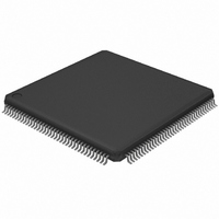
LPC2210FBD144/01,5 NXP Semiconductors, LPC2210FBD144/01,5 Datasheet - Page 18

LPC2210FBD144/01,5
Manufacturer Part Number
LPC2210FBD144/01,5
Description
IC ARM7 MCU 16KRAM W/ADC 144LQFP
Manufacturer
NXP Semiconductors
Series
LPC2200r
Datasheet
1.LPC2210FBD144015.pdf
(50 pages)
Specifications of LPC2210FBD144/01,5
Program Memory Type
ROMless
Package / Case
144-LQFP
Core Processor
ARM7
Core Size
16/32-Bit
Speed
60MHz
Connectivity
EBI/EMI, I²C, Microwire, SPI, SSI, SSP, UART/USART
Peripherals
POR, PWM, WDT
Number Of I /o
76
Ram Size
16K x 8
Voltage - Supply (vcc/vdd)
1.65 V ~ 3.6 V
Data Converters
A/D 8x10b
Oscillator Type
Internal
Operating Temperature
-40°C ~ 85°C
Processor Series
LPC22
Core
ARM7TDMI-S
Data Bus Width
16 bit, 32 bit
Data Ram Size
16 KB
Interface Type
I2C/SPI/SSP/UART
Maximum Clock Frequency
60 MHz
Number Of Programmable I/os
76
Number Of Timers
2
Operating Supply Voltage
3.3 V
Maximum Operating Temperature
+ 85 C
Mounting Style
SMD/SMT
3rd Party Development Tools
MDK-ARM, RL-ARM, ULINK2
Minimum Operating Temperature
- 40 C
On-chip Adc
8-ch x 10-bit
Lead Free Status / RoHS Status
Lead free / RoHS Compliant
For Use With
OM10091 - KIT DEV PHYCORE-ARM7/LPC2220622-1005 - USB IN-CIRCUIT PROG ARM7 LPC2K568-1757 - BOARD EVAL FOR LPC220X ARM MCU
Eeprom Size
-
Program Memory Size
-
Lead Free Status / Rohs Status
Lead free / RoHS Compliant
Other names
568-4012
935282078551
LPC2210FBD144/01-S
935282078551
LPC2210FBD144/01-S
Available stocks
Company
Part Number
Manufacturer
Quantity
Price
Company:
Part Number:
LPC2210FBD144/01,5
Manufacturer:
NXP Semiconductors
Quantity:
10 000
NXP Semiconductors
LPC2210_2220_6
Product data sheet
6.5 Pin connect block
6.6 Pin function select register 0 (PINSEL0 - 0xE002 C000)
The pin connect block allows selected pins of the microcontroller to have more than one
function. Configuration registers control the multiplexers to allow connection between the
pin and the on chip peripherals. Peripherals should be connected to the appropriate pins
prior to being activated, and prior to any related interrupt(s) being enabled. Activity of any
enabled peripheral function that is not mapped to a related pin should be considered
undefined.
The pin control module contains three registers as shown in
Table 6.
The PINSEL0 register controls the functions of the pins as per the settings listed in
Table
function is selected for a pin. For other functions, direction is controlled automatically.
Settings other than those shown in
Table 7.
Address
0xE002 C000
0xE002 C004
0xE002 C014
PINSEL0
1:0
3:2
5:4
7:6
9:8
7. The direction control bit in the IODIR register is effective only when the GPIO
Pin control module registers
Pin function select register 0 (PINSEL0 - 0xE002 C000)
Pin name
P0.0
P0.1
P0.2
P0.3
P0.4
Name
PINSEL0
PINSEL1
PINSEL2
Rev. 06 — 11 December 2008
Value
0
0
1
1
0
0
1
1
0
0
1
1
0
0
1
1
0
0
1
1
0
1
0
1
0
1
0
1
0
1
0
1
0
1
0
1
0
1
0
1
Table 7
Description
pin function select register 0
pin function select register 1
pin function select register 2
are reserved, and should not be used
Function
GPIO Port 0.0
TXD0 (UART0)
PWM1
reserved
GPIO Port 0.1
RXD0 (UART0)
PWM3
EINT0
GPIO Port 0.2
SCL (I
Capture 0.0 (Timer 0)
reserved
GPIO Port 0.3
SDA (I
Match 0.0 (Timer 0)
EINT1
GPIO Port 0.4
SCK (SPI0)
Capture 0.1 (Timer 0)
reserved
2
2
C-bus)
C-bus)
16/32-bit ARM microcontrollers
LPC2210/2220
Table
6.
Value after reset
0
0
0
0
0
© NXP B.V. 2008. All rights reserved.
Access
read/write
read/write
read/write
18 of 50


