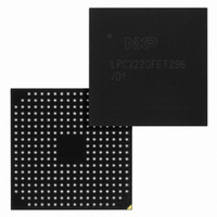
LPC3220FET296/01,5 NXP Semiconductors, LPC3220FET296/01,5 Datasheet - Page 10

LPC3220FET296/01,5
Manufacturer Part Number
LPC3220FET296/01,5
Description
IC ARM9 MCU 128K 296-TFBGA
Manufacturer
NXP Semiconductors
Series
LPC32x0r
Specifications of LPC3220FET296/01,5
Package / Case
296-TFBGA
Core Processor
ARM9
Core Size
16/32-Bit
Speed
266MHz
Connectivity
EBI/EMI, I²C, IrDA, Microwire, SPI, SSI, SSP, UART/USART, USB OTG
Peripherals
DMA, I²S, Motor Control PWM, PWM, WDT
Number Of I /o
51
Program Memory Type
ROMless
Ram Size
128K x 8
Voltage - Supply (vcc/vdd)
0.9 V ~ 3.6 V
Data Converters
A/D 3x10b
Oscillator Type
Internal
Operating Temperature
-40°C ~ 85°C
Processor Series
LPC32
Core
ARM926EJ-S
Data Bus Width
32 bit
Data Ram Size
128 KB
Interface Type
EMC
Maximum Clock Frequency
266 MHz
Number Of Timers
6
Operating Supply Voltage
1.31 V to 1.39 V
Maximum Operating Temperature
+ 85 C
Mounting Style
SMD/SMT
3rd Party Development Tools
MDK-ARM, RL-ARM, ULINK2
Minimum Operating Temperature
- 40 C
On-chip Adc
10 bit, 3 Channel
Lead Free Status / RoHS Status
Lead free / RoHS Compliant
Eeprom Size
-
Program Memory Size
-
Lead Free Status / Rohs Status
Lead free / RoHS Compliant
Other names
568-4965
935290763551
935290763551
Available stocks
Company
Part Number
Manufacturer
Quantity
Price
Company:
Part Number:
LPC3220FET296/01,5
Manufacturer:
NXP Semiconductors
Quantity:
10 000
NXP Semiconductors
ES_LPC3220
Errata sheet
3.4 DDR.1: DDR interface has >1.2 ns clock skew
Introduction:
DDR memory uses a differential clock which is generated by the LPC3220. The
differential clock consists of two clock signals: EMC_CLK is the positive clock and
DDR_nCLK is the negative clock.
Problem:
There is approximately 1.27 ns of skew between the low transition of the DDR_nCLK and
the high transition of the EMC_CLK. This can cause two problems: 1) Some DDR devices
use this clock transition to drive a digital lock loop (DLL) in the DDR device. The DDR
clock skew can cause the DDR device's internal DLL to loose lock, resulting in the wrong
data being latched. 2) The DDR clock skew can also cause a reduced Data Valid Window
(also called Data-Out Window) from a DDR device. However, the LPC3220 has a
programmable DQS delay to achieve center alignment for accurate data reads.
Work-around:
Connecting the DDR device negative clock input (DDR_nCLK from the LPC3220) to the
DDR Reference Voltage (Vref - the midpoint of the DDR signal voltage swing, which is
generally VDDQ/2) avoids the clock skew problem, though it also eliminates the
advantages of differential signaling. The LPC3220 DDR_nCLK output should be left
unconnected. DDR Reference Voltage can be generated with a divide-by-two voltage
divider. Standard DDR memories usually require a Vref input, so this DDR reference
voltage should already be available. Mobile DDR devices typically do not have a Vref
input, so the external voltage divider may need to be added to the design for this
work-around.
It is also possible to compensate for the 1.27 ns clock skew by adding an additional
7 inches of pcb trace length to the EMC_CLK signal. However, this could have
unintentional consequences; such as increased Electro-Magnetic Interference.
All information provided in this document is subject to legal disclaimers.
Rev. 8 — 1 February 2011
ES_LPC3220
Errata sheet LPC3220
© NXP B.V. 2011. All rights reserved.
10 of 16


